Make pins follow the transmit samples
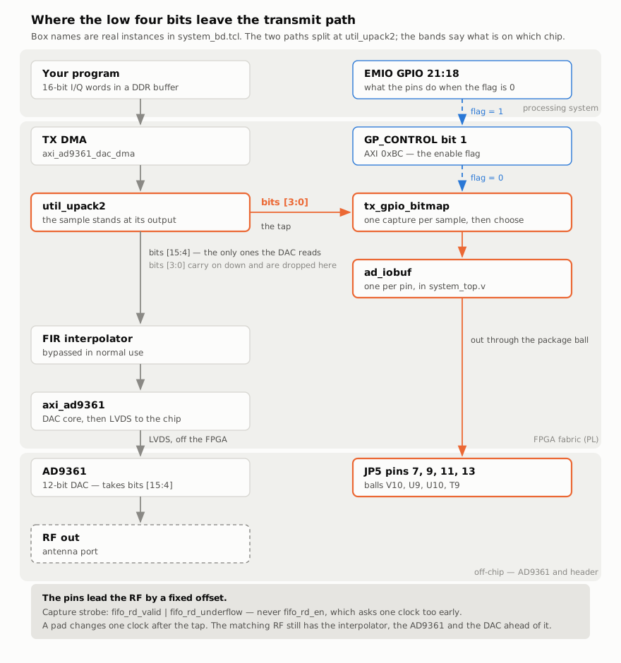
Turn on tx_sample_gpio_en, and JP5 pins 7, 9, 11 and 13 carry the low
four bits of every transmitted I sample on channel 0. The AD9361's DAC takes
only the top 12 of your 16 bits, so those four bits cost no analog
performance. The pattern you put in them is the clock, trigger or marker.
# run from: the board. Resolve the device by name; the iio:deviceN index is not stable
D=$(for d in /sys/bus/iio/devices/iio:device*; do
      [ "$(cat $d/name)" = cf-ad9361-dds-core-lpc ] && echo $d; done)

cat   $D/tx_sample_gpio_en                # 0 = GPIO, 1 = sample nibble
echo 1 > $D/tx_sample_gpio_en             # on
echo 0 > $D/tx_sample_gpio_en             # off
From the host: iio_attr -u ip:192.168.2.1 -d cf-ad9361-dds-core-lpc tx_sample_gpio_en 1
(use -d, not -c). The register resets to 0, so the pins are ordinary GPIO
at power-on.
The pattern is data
| Rule | |
|---|---|
| OR the nibble in last | after every scaling, gain or format conversion, or those steps overwrite it |
| Only channel 0's I samples carry it | |
| Cyclic buffer = continuous clock | make the buffer length an exact multiple of the pattern period, or there is a glitch at the wrap |
| Fastest toggle | half the sample rate: 30.72 MHz at 61.44 MSPS |
| GNU Radio | a complex float flowgraph destroys the low bits; work at short end to end |
The complete program, step by step:
write a pin pattern in Python.
tools/sample_gpio_clock.py is the same
program with arguments and teardown on Ctrl-C.
It works with the transmitter muted, but opening a buffer can unmute it
Opening a TX buffer can itself raise the attenuator (seen at −61.5 dB on a board reading −89.75). Mute after the buffer starts, read both attenuators back, and mute before tearing the buffer down (before you transmit).
Never engage the FPGA's ÷8 transmit interpolator
It does not work on this board: a tone sent through it does not come out at
all. You reach it only by setting the DAC core's
out_voltage_sampling_frequency to one eighth of the AD9361's rate yourself.
Check it on your board
No scope, jumper or antenna needed; TX attenuation stays at maximum:
# run from: the repo root, on your host
./tools/tx-gpio-bitmap-check.py ip:fishball.local
You should see: every nibble line end in ok.
| Measured (Saleae Logic 8) | |
|---|---|
| full rate, pin 0 at 30.72 MHz from 61.44 MSPS | every sample present |
| the four pins switch together | within 1.5 ns |
| pins vs RF | the pins lead the RF by about a microsecond, designed-for, not measured: never treat a pin edge and its RF as simultaneous |
Reference: sample-locked GPIO: how it is built, limits, measurements.