What is on the board
The board's main parts, clocks, connectors and supply rails, read off the
vendor schematic in docs/vendor/ (sheet
numbers given) and cross-checked against a running board where possible. For
the tasks, see which port is which,
use an external reference clock and
find a part on the schematic.
What it looks like
Sold bare or boxed. Boxed, as the PlutoSky R1, it is a black aluminium case with a
fan on top: the Ethernet jack and two USB-C sockets at one end, labelled ETH,
DEBUG and USB, the four SMA connectors at the other, and the JP5 GPIO
header reachable through a slot beside the fan.
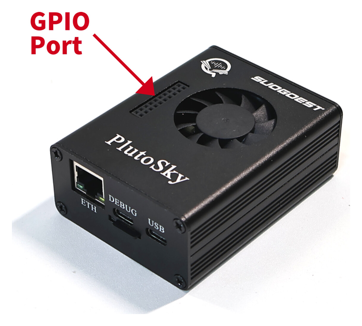
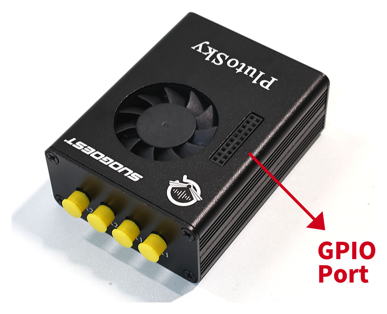
Case photos: OpenSourceSDRLab's product pages. The board photo below is the vendor's too.
On some PlutoSky R1 units the case's SMA labels are in the wrong order
What is printed on the case does not match the ports on the board behind
it. Trust the board, not the box: with the lid off, each SMA has its name,
TX1A, RX1A, TX2A or RX2A, on the silkscreen beside it. To check a
unit without opening it, and why it matters most in a loopback, see
which port is which.
What is where
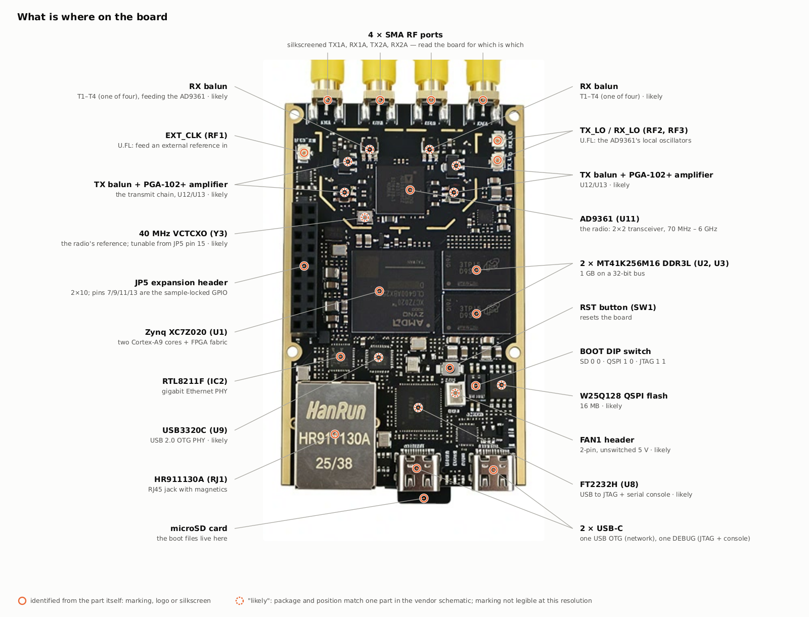
Solid ring: identified from its marking. Dashed ring, "likely": only the package
and position fit. Regenerated by docs/img/make_board_map_svg.py.
The main devices
| Ref | Part | What it does | Sheet | Corroborated by | Datasheet |
|---|---|---|---|---|---|
U1 |
Xilinx XC7Z020-CLG400 | Zynq-7000: two Cortex-A9 cores plus Artix-7 fabric | 1, 2, 3, 5, 6 | legible on the package | DS187 · DS190 overview |
U2 U3 |
Micron MT41K256M16TW-107IT:P | DDR3L, 4 Gbit ×16 each, so 1 GB across a 32-bit bus | 3 | Micron logo and FBGA code D9SHD legible; board reports MemTotal: 1027848 kB |
Micron part page |
U11 |
Analog Devices AD9361 | the radio: 2×2 transceiver, 70 MHz – 6 GHz | 10, 11, 12 | ADI logo legible; ad9361-phy in IIO |
AD9361 |
U12 U13 |
Mini-Circuits PGA-102+ | transmit power amplifier, one per channel | 12 | SOT-89 packages beside the outer SMA ports; self-test measures ~15.7 dB of gain at 900 MHz | PGA-102+ |
T1–T4 |
RF baluns (the schematic gives no part number) | single-ended SMA ↔ the AD9361's differential RF pins, one per port. On transmit the balun is before the amplifier: AD9361 TX1A_P/N → T1 → TX1A_I → U12 → TX1A_O → SMA |
12 | four square 6-pad parts around the AD9361; pads labelled PRIMARY, PRIMARY_DOT, SECONDARY_DOT, NOT_USED, GND, a transformer footprint with polarity dots |
— |
U8 |
FTDI FT2232HL | USB to JTAG and serial console, on one socket | 8 | two ttyUSB ports enumerate together |
FT2232H |
U9 |
Microchip USB3320C-EZK | USB 2.0 OTG PHY | 9 | the usb0 network interface |
USB3320 |
IC2 |
Realtek RTL8211F-CG | gigabit Ethernet PHY | 4 | Realtek logo legible; eth0 |
Realtek product page |
RJ1 |
HanRun HR911130A | RJ45 with integrated magnetics | 4 | legible on the part | LCSC page, with datasheet |
| — | Winbond W25Q128JVSIQ | 16 MB QSPI flash: FSBL, U-Boot, its environment, a small Linux image | 2 | four MTD partitions totalling 16 MB | W25Q128JV |
IC1 |
onsemi MAX809TTRG | reset supervisor, behind the RST button (SW1) |
2 | MAX809 | |
IC7 |
TI TXS02612RTWR | SD-card level shifter and 2-port expander | 7 | TXS02612 | |
IC4 |
serial EEPROM (inferred) | holds the FT2232's USB descriptors; the schematic shows EEDAT, DI, DO against the FT2232 |
8 | — | |
K1 Q3 |
Panasonic AQY221N2VW solid-state relay + AOS AO3400A MOSFET | the PTT switch, brought out on JP5 pin 17 | 13 | AQY221N2VW · AO3400A |
The power regulators are not in the published schematic, so this page cannot name them.
The baluns (balanced-to-unbalanced transformers) set the board's usable
frequency range, not the AD9361. With no part number, only a measurement can
say where the range ends; the known figure is that
loop gain is flat to 2 dB from 200 MHz to 1 GHz. Each
port also has its own fixed phase offset, so the two channels are coherent but
not phase-calibrated: measure phase with a splitter and matched cables. The
AD9361's RX1B/RX2B pairs are not wired; the four SMAs are the A ports.
Clocks
| Ref | Frequency | Feeds | Sheet |
|---|---|---|---|
Y3 |
40 MHz | the AD9361 reference: a 4-pin oscillator whose output goes through R107 (33 Ω) to the AD9361's XTALN (ball M12), DC-coupled. Its pin 1, on a net named XTAL_VTC, is brought out on JP5 pin 15; the schematic symbol calls that pin OE, so whether it tunes the frequency or switches the output off is unconfirmed (below) |
10 |
Y2 |
33.333 MHz | PS_CLK, the Zynq processing system |
6 |
Y1 |
50 MHz | the PL fabric, at 1.8 V | 5 |
OS1 |
25 MHz | the Ethernet PHY | 4 |
OS2 |
24 MHz | the USB PHY | 9 |
X1 |
crystal, with 18 pF loading caps | the FT2232HL | 8 |
Everything the AD9361 does derives from Y3, so its accuracy is the radio's.
Connectors
| Ref | What it is |
|---|---|
| 4 × SMA | TX1A, RX1A, TX2A, RX2A. Read the silkscreen rather than counting positions, or the labels on the case, which are wrong on some units |
RF1 |
EXT_CLK, U.FL. Connected to nothing as shipped. Moving R107's 33 Ω to R109 makes it the radio's reference input; R110 would take it to the FPGA (Zynq pin K17). See locking to an external reference |
RF2 RF3 |
TX_LO and RX_LO, U.FL: the AD9361's local oscillators, brought out |
JP5 |
the 2×10 expansion header. Pins 7/9/11/13 are sample_gpio[3:0]; see the pinout |
JP1–JP4 |
further headers |
BOOT1 |
the 2-position boot switch: SD 0 0, QSPI 1 0, JTAG 1 1 |
RJ1, 2 × USB-C, microSD, FAN1 |
network, host connections, boot media, fan |
RED1 BLUE1 |
the two LEDs, each through 240 Ω |
Locking the board to an external reference
To feed the radio an external reference through EXT_CLK, move the 33 Ω
resistor from R107 to R109: unsolder it from R107, solder it (or a new
33 Ω of the same size) across R109's empty pads. R107 cuts Y3 off the radio's
reference line; R109 joins that line to the EXT_CLK U.FL socket. As
shipped, EXT_CLK is connected to nothing. Unlike the Rev.C ADALM-Pluto, which
selects its reference with a GPIO (refclk_source in U-Boot), this board has
no switch: the resistors are the switch.
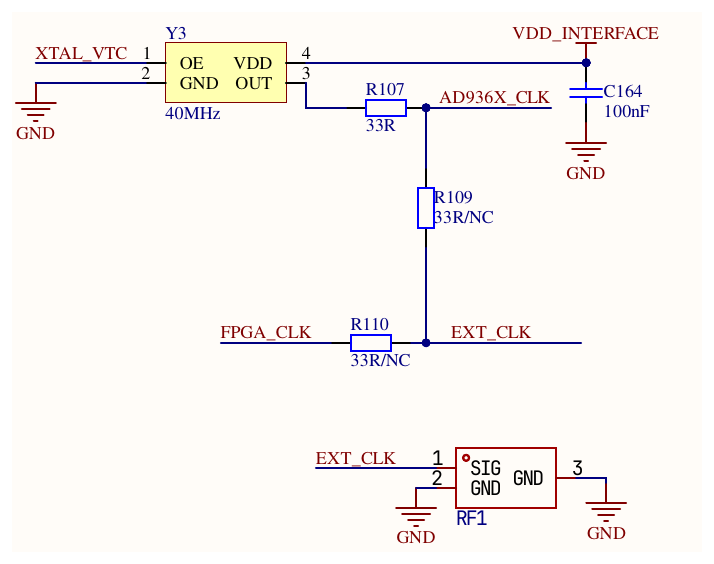
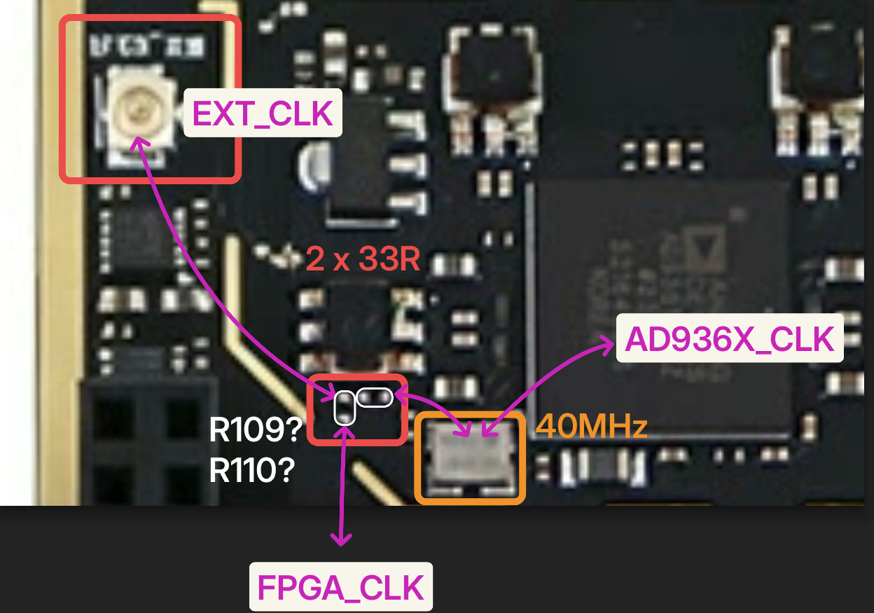
The footprints beside Y3: their shared pad is EXT_CLK; the horizontal
pair, towards Y3, is R109; the vertical pair R110. The photo is the
vendor's, enlarged: confirm with a continuity check before fitting anything.
The parts
| Part | Joins | As shipped |
|---|---|---|
R107 33 Ω |
Y3's output to AD936X_CLK, the AD9361's XTALN (ball M12) |
fitted |
R109 33R/NC |
AD936X_CLK to EXT_CLK (RF1, U.FL) |
empty |
R110 33R/NC |
EXT_CLK to FPGA_CLK, Zynq pin K17 (not constrained in the stock design) |
empty |
C164 100 nF |
Y3's supply (VDD_INTERFACE) to ground |
fitted. Decoupling, not a series capacitor: the reference line is DC-coupled |
The configurations
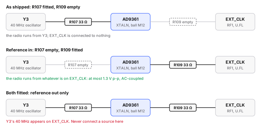
R107 |
R109 |
The radio's reference | EXT_CLK |
Measured on this board |
|---|---|---|---|---|
| fitted | empty | Y3, 40 MHz |
nothing | stock: 40.0001 MHz, every lock held under stress |
| empty | fitted | whatever is on EXT_CLK |
reference in | with nothing on EXT_CLK the radio does not start (below) |
| fitted | fitted | Y3 |
Y3's 40 MHz, out |
a HackRF CLKOUT on EXT_CLK changed nothing: Y3 out-drives it |
- Never connect a source to
EXT_CLKwith both fitted. Two outputs then drive one line through 66 Ω. As a reference output (to lock another instrument to this board) it works, but the cable hangs on the radio's own reference line: keep it short, or buffer it. R110putsEXT_CLKon an FPGA clock pin instead, or as well. Fabric logic could then count the AD9361's data clock against it: measureY3, timestamp samples, or close a disciplining loop. Nothing in the stock design uses it.
Feeding a reference in
With R107 moved to R109:
| Requirement | Why |
|---|---|
| 10 to 80 MHz | the AD9361's external-reference range |
| At most 1.3 V p-p, AC-coupled (AD9361 datasheet) | XTALN sits in the chip's 1.3 V analogue domain; R109 alone provides no coupling capacitor and no attenuation |
| Running before the board boots | the driver locks the BBPLL once, at 1.4 s into boot |
clock-frequency in the device tree equal to it, unless it is 40 MHz |
the driver programs every PLL from that number (node /clocks/clock@0, ad9364_clkin, in zynq-pluto-sdr.dtsi; flash with ./devkit flash --dtb-only). U-Boot's ad936x_ext_refclk_override would do it without a rebuild, but only the QSPI and DFU boot paths apply it, not the SD-card boot this firmware uses |
Without a reference, the radio does not start. Measured with R107
removed and nothing driving EXT_CLK: ad9361 spi0.0: Calibration TIMEOUT
(0x5E, 0x80), then probe with driver ad9361 failed with error -110;
fishball-rf-quiesce fails and iiod is held back, so nothing can transmit.
Refitting R107 brings it back.
A 3.3 V CMOS source needs a DC block and about 20 dB. XTALN is a
high-impedance load, not 50 Ω, so a 50 Ω attenuator divides much less than
its rating:
| 50 Ω pad into a high-impedance load | 3.3 V p-p becomes |
|---|---|
| 6 dB | about 2.6 V p-p |
| 10 dB | about 1.9 V p-p |
| 20 dB | about 0.65 V p-p |
From an open-circuit calculation; check the real swing on a scope.
HackRF One as the reference. Its CLKOUT is a 10 MHz, 3.3 V square wave,
off after every power-up. Turn it on before the Fishball boots, and set the
device tree to <10000000>:
# run from: the PC the HackRF is plugged into
hackrf_clock -o 1      # CLKOUT on (10 MHz)
hackrf_clock -r 2      # on HackRF One r9, CLKOUT is Si5351 clock 2: "Up" means on
hackrf_clock --help gives -r 3 as the CLKOUT example; that is the older
boards' layout. The HackRF's CLKIN accepts only 10 MHz, so Y3's 40 MHz cannot
drive it the other way.
Which reference is the radio really using
The settings alone do not tell you: a board whose reference was not what its device tree said still reported every PLL locked. Two checks (step by step):
# run from: the board
D=/sys/kernel/debug/iio/iio:device0
for r in 0x05E 0x247 0x287; do echo $r > $D/direct_reg_access; echo "$r $(cat $D/direct_reg_access)"; done
#   0x05E 0x81   bit 7: BBPLL locked
#   0x247 0x2    bit 1: RX synthesizer locked
#   0x287 0x2    bit 1: TX synthesizer locked
The frequency itself: stream at 20 MS/s on the board (iio_readdev -u local:)
and time the samples against CLOCK_MONOTONIC_RAW, the Zynq's own 33.333 MHz
crystal. Use the RAW clock: right after boot, network time slews
CLOCK_MONOTONIC, and a stock board read −93 ppm instead of +2. Over 120 s
this resolves a few ppm, enough to tell a 40 MHz reference from a 10 MHz one,
not to discipline one.
Without soldering
-
xo_correction: the frequency, not the source. MeasureY3against a disciplined reference and write its true frequency; the PLLs are then programmed from it. Accuracy, not stability.# run from: the board cat /sys/bus/iio/devices/iio:device0/xo_correction_available # [39992000 1 40008000] min, step, max -> 1 Hz steps, about 0.025 ppm cat /sys/bus/iio/devices/iio:device0/xo_correction # 40000000 -
Y3's pin 1 (XTAL_VTC, JP5 pin 15): OE or tuning input, unconfirmed. The schematic symbol calls it OE; the net name suggests a tuning voltage. If it is an enable, holding it low stopsY3, and fittingR109alone (withR107left in) would make the reference switchable, as on the Rev.C Pluto. The marking onY3, or the pin's voltage at rest (near the supply for an enable, near mid-supply for a tuning input), settles it. Measure before driving it: a jumper to ground there survives a reboot, and as an enable it leaves the radio without a clock.
Supply rails
From sheet 1: VCC5V, VCC3V3, VCC1V8, VCC1V35 (the DDR3L bank) and 1V3_A (the AD9361's analogue supply). Bank 13, where the sample-locked GPIO pins live, runs from VCC3V3; the evidence is under the pins.
What this page cannot tell you
- Which physical SMA or USB-C socket is which: that is in the PCB layout, which this repo does not have. Read the silkscreen, not the case labels, which are wrong on some units. Use both USB-C sockets, one on a mains charger: on laptop bus power alone the board browns out under sustained use (troubleshooting).
- Whether
RF1/RF2/RF3are fitted on your board: options such asR109andR110(33R/NC) are the kind of thing that differs between production runs. Look first. - Most passive component values: they are in the schematic.