Find a part on the schematic
Use docs/vendor/7020_936x_SDR-schematic.pdf:
13 pages, created 15 February 2025. Every pin claim in this repository comes
from it.
Do not use the vendor's GitHub copy
hardware/schematic_PlutoSky.pdf on the vendor's GitHub is a different board
revision: 15 pages, May 2025, no JP5, no 3V3_IO1..4, connectors numbered
J1–J12.
| Sheet | What it settles |
|---|---|
| 1 | VCCO_13_1..4 tie to VCC3V3: why bank 13 is LVCMOS33 |
| 5 | which FPGA ball carries which 3V3_IO net, and which nearby balls are no connect |
| 10 | the AD9361 and its 40 MHz reference, Y3 |
| 13 | connector JP5: which header pin carries which net; GND on pins 2 and 20 |
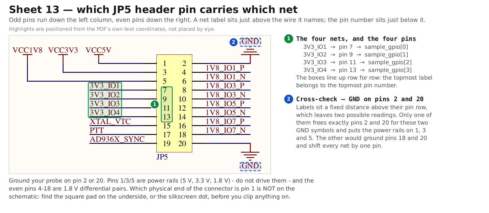
Sheet 13, annotated: the kind of evidence each pin claim rests on. The crops of sheets 1, 5 and 13 are in the GPIO reference.
The main parts
| Ref | Part | Sheet |
|---|---|---|
U1 |
Xilinx XC7Z020-CLG400: two Cortex-A9 cores plus Artix-7 fabric | 1, 2, 3, 5, 6 |
U2 U3 |
Micron MT41K256M16TW-107IT:P, DDR3L: 1 GB together | 3 |
U11 |
Analog Devices AD9361: 2×2 transceiver, 70 MHz – 6 GHz | 10, 11, 12 |
U12 U13 |
Mini-Circuits PGA-102+: transmit power amplifier, one per channel | 12 |
T1–T4 |
RF baluns (no part number): they set the usable frequency range | 12 |
U8 |
FTDI FT2232HL: USB to JTAG and serial console | 8 |
IC2 |
Realtek RTL8211F-CG: gigabit Ethernet PHY | 4 |
The ratings everything is checked against
| AD9361 Data Sheet, Rev. G, Table 11 | |
|---|---|
| RF Inputs (Peak Power) | 2.5 dBm: nothing may reach a receive input above this |
| Maximum Junction Temperature | 110 °C (150 °C is the storage maximum, a different row) |
Reference: what is on the board (every part, with datasheets) · vendor documents (provenance, checksum, the Zynq temperature grades).