Two receivers that both survive decimation
With the FPGA's ÷8 decimator engaged, upstream's block design filters only
channel 0, so channel 1 comes out aliased. Patch
firmware/patches/0021-filter-both-receive-channels-by-default.patch puts both
channels through the filter for about six lines of Tcl and 22 DSP slices; it is
applied by every build. This page records the defect, the measurements and
the cost. To capture both channels, see
receive on both channels.
- the defect (upstream): with the ÷8 decimator engaged, channel 1 is sampled at one eighth rate with no anti-alias filter: a 10 MHz tone's alias lands at 2.32 MHz at full strength
- the fix: patch
0021, applied by every build: both channels through the filter - result: at least 69.7 dB of alias suppression on channel 1
- cost: 22 DSP slices (94 / 220 instead of 72 / 220); timing still met
- not fixed: the transmit interpolator: do not engage it, TX1 then emits nothing
Using it
Nothing to do: ./devkit setup --target factory applies it with the rest of the patch series.
Engage the decimator and capture both channels:
# run from: your host
iio_attr -u ip:192.168.2.1 -i -c cf-ad9361-lpc voltage0 sampling_frequency_available
#   61440000 7680000        <- always {converter rate, converter rate / 8}

iio_attr -u ip:192.168.2.1 -i -c cf-ad9361-lpc voltage0 sampling_frequency 7680000

# channel 0 is voltage0/voltage1, channel 1 is voltage2/voltage3
iio_readdev -u ip:192.168.2.1 -b 131072 -s 262144 cf-ad9361-lpc \
  voltage0 voltage1 voltage2 voltage3 > both.bin
To build upstream's wiring instead (channel 0 filtered, channel 1 straight
through, 22 DSP slices back), delete the Vivado project (or the build reuses it)
and set STOCK_RX_FILTER=1. An empty STOCK_RX_FILTER= counts as unset.
# run from: the repo root
rm -rf firmware/src/hdl/projects/pluto/pluto.{xpr,cache,gen,hw,ip_user_files,runs,sim,srcs,sdk}
STOCK_RX_FILTER=1 ./devkit build --target factory --hdl-only && ./devkit verify --target factory \
  && ./devkit flash --target factory --boot-only
system_bd.tcl prints which wiring it chose, and ./devkit verify --target factory reports
-> decimator on RX channel 0 only (STOCK_RX_FILTER=1, upstream wiring) or
-> decimator on BOTH RX channels (default).
The defect
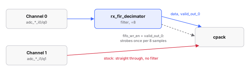
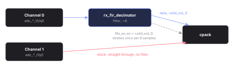
Three facts in the stock block design combine badly:
- Only channel 0 is filtered. Channel 1 goes straight to
cpackinputs 2 and 3. cpackcaptures everything on channel 0's timing. Its write strobe,fifo_wr_en, isrx_fir_decimator/valid_out_0; channel 1'sadc_valid_i1is connected to nothing.- The decimator drops the rate by 8, so that strobe fires once per eight input samples.
So channel 1 is sampled at one eighth rate with no anti-alias filter: everything outside ±Fs/16 folds onto it, offset from channel 0 by the filter's group delay. Keeping one sample in eight folds eight slices of bandwidth (noise included) on top of each other; the FIR empties the seven discarded slices first, which is also where decimation's 10·log₁₀(D) dB of signal-to-noise gain comes from. Upstream shares this design with many 1R1T boards (one receiver, one transmitter), where the asymmetry never shows.
Before and after
TX2A → 20 dB attenuator → RX2A, 900 MHz, converter at 61.44 MSPS, decimator
engaged (7.68 MSPS, a ±3.84 MHz window). A tone generated in the FPGA is swept
0.2–20 MHz and compared with the same tone with the decimator bypassed: the
difference is the channel's anti-alias response.
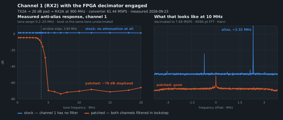
| Tone | Folds in at | Stock | With this patch |
|---|---|---|---|
| 1.00 MHz | 1.00 MHz, in band | +1.4 dB | −4.6 dB |
| 3.84 MHz | 3.84 MHz, the edge | +1.4 dB | −10.6 dB |
| 5.00 MHz | −2.68 MHz | +1.4 dB | −69.6 dB |
| 10.00 MHz | +2.32 MHz | +1.4 dB | −70.4 dB |
| 20.00 MHz | −3.04 MHz | +1.2 dB | −66.0 dB |
Stock, channel 1 attenuates nothing, so every tone above 3.84 MHz lands in the window at full strength: the 10 MHz tone's alias at 2.32 MHz peaks at +18.75 dB, indistinguishable from a real signal. Patched, the alias is invisible (at least 69.7 dB of suppression; average −70.1 dB past 5 MHz). With the decimator bypassed the two builds agree within 0.05 dB.
What the patch does
The Tcl helper (projects/common/xilinx/adi_fir_filter_bd.tcl) already loops
over its channel count, so the fix asks for four and wires the second pair:
# excerpt: the patch's change to projects/pluto/system_bd.tcl
# ask for 4 (ch0 I/Q and ch1 I/Q) rather than 2
ad_add_decimation_filter "rx_fir_decimator" 8 4 1 {61.44} {61.44} <coe>

# feed channel 1 in
ad_connect axi_ad9361/adc_valid_i1  rx_fir_decimator/valid_in_2
ad_connect axi_ad9361/adc_enable_i1 rx_fir_decimator/enable_in_2
ad_connect axi_ad9361/adc_data_i1   rx_fir_decimator/data_in_2
ad_connect axi_ad9361/adc_valid_q1  rx_fir_decimator/valid_in_3
ad_connect axi_ad9361/adc_enable_q1 rx_fir_decimator/enable_in_3
ad_connect axi_ad9361/adc_data_q1   rx_fir_decimator/data_in_3

# and take cpack's inputs from the filter instead of from axi_ad9361
ad_connect cpack/enable_2        rx_fir_decimator/enable_out_2
ad_connect cpack/fifo_wr_data_2  rx_fir_decimator/data_out_2
ad_connect cpack/enable_3        rx_fir_decimator/enable_out_3
ad_connect cpack/fifo_wr_data_3  rx_fir_decimator/data_out_3
Both channels now share one active bit, one coefficient set and one group
delay, so they stay sample-aligned and cpack/fifo_wr_en on valid_out_0 is
correct.
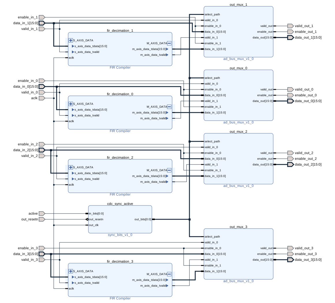
Four fir_compilers and four bypass muxes instead of two, with one
cdc_sync_active driving every select_path, so both channels switch together.
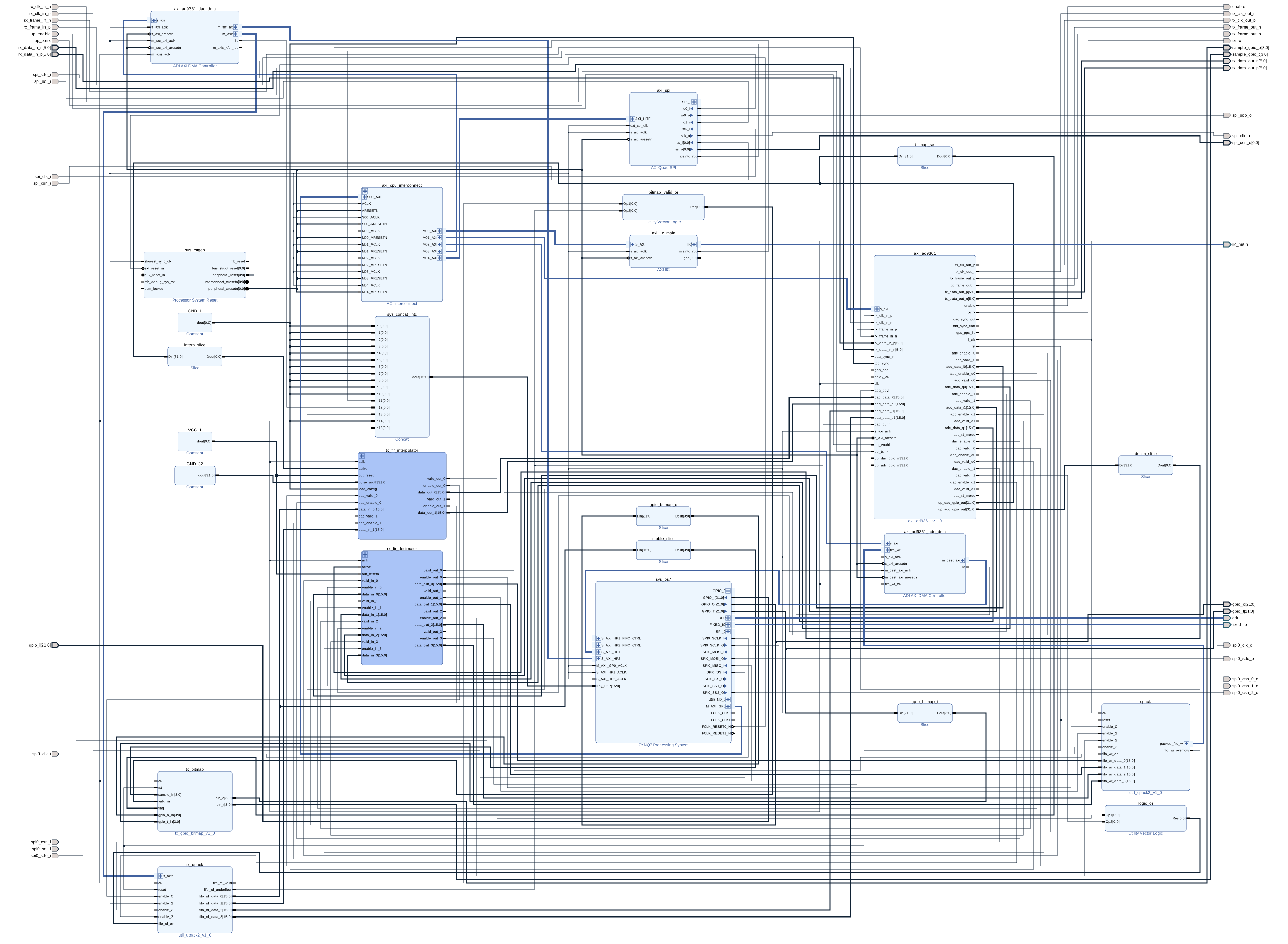
The whole design is img/bd-top.svg; both drawings come from
img/make_bd_layout.sh.
What it costs
STOCK_RX_FILTER=1 |
Default | |
|---|---|---|
| DSP48 slices | 72 / 220 | 94 / 220 |
| Slice LUTs | 11,896 / 53,200 | 12,521 / 53,200 |
| Worst negative slack | +0.205 ns | +0.215 ns |
| Timing endpoints | 48,263 | 54,211 |
Two extra fir_compiler instances, about 11 DSP slices each; timing is met with
slightly more margin than stock, and 126 DSP slices remain free.
What this does not fix
The transmit interpolator: do not engage it
tx_upack/fifo_rd_en is the OR of the interpolator's valid and channel 1's DAC
valid, so on a 2R2T board channel 1 drags the packer at full rate and TX1 emits
nothing. See block-design.md.
- The shared coefficient file. Receive and transmit both use
library/util_fir_int/coefile_int.coe; editing it changes both. - The ÷8 factor. The driver offers exactly
{1, 8}; another rate would build and be unreachable.