The stock block design: what's in it, how it connects, what you can change
A reference to the Vivado design the devkit builds: every block, clock, address
and trap. It is generated by firmware/src/hdl/projects/pluto/system_bd.tcl
(with system_top.v and system_constr.xdc beside it, once setup.sh has
run). Read it before changing HDL: most of the traps are in how the pieces are
wired, not in any one piece. To make a change, follow
add your own logic to the FPGA. Terms are defined in
the glossary at the end.
A sample's journey
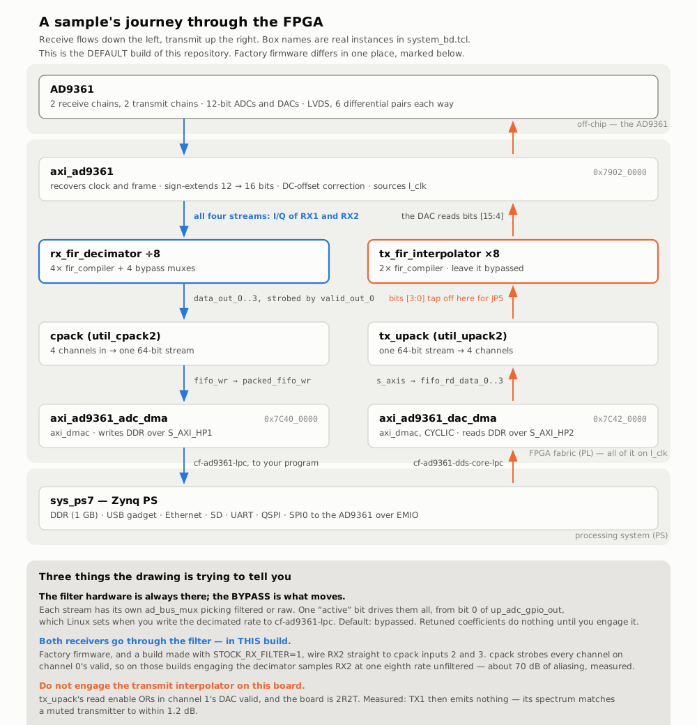
Redraw with docs/img/make_datapath_svg.py. Its
counts come from the generated system.bd, not system_bd.tcl, which carries
both receive wirings behind an if.
| Stage | What happens |
|---|---|
| AD9361 | mixes the antenna signal to baseband and digitises it: 12-bit I and Q for each of two receive channels |
| LVDS | the samples cross to the FPGA, six differential lanes each way |
axi_ad9361 |
recovers clock and frame, sign-extends 12 to 16 bits, corrects DC offset, and outputs four streams (I/Q of channel 0 and 1) |
rx_fir_decimator |
all four streams enter this ÷8 filter, with one bypass mux per stream and one shared active bit. It is bypassed by default |
cpack |
packs the enabled channels into one 64-bit stream |
| DMA | writes it into DDR; Linux's IIO subsystem serves it as cf-ad9361-lpc |
Everything in the datapath runs on l_clk, the AD9361's own data clock,
whose rate follows the sample rate. Any block inserted between axi_ad9361 and
the packers lives in that domain.
Both receivers are symmetric on the default build, not on factory firmware.
Upstream sends channel 1 straight to cpack; this repository routes both
through the filter (patch 0021). STOCK_RX_FILTER=1 rebuilds upstream's
version, and ./devkit verify --target factory reports which a bitstream has. See
both-receive-channels.md.
Transmit is the reverse, with one asymmetry: receive samples are right-aligned (12 bits sign-extended into 16), transmit samples are MSB-aligned (the DAC takes the top 12 bits). Transmit scaled to ±2047 comes out 24 dB quiet; scale to ±32767. The discarded bottom four bits drive the sample-locked GPIO outputs.
The IP blocks, one by one
sys_ps7 — the Zynq processing system
Xilinx processing_system7: the two ARM cores and every hard peripheral. DDR
controller (MT41K256M16, 32-bit, 1 GB), USB0 (the gadget), ENET0 (RJ45), SD0
(boot), UART1 (console), QSPI (16 MiB flash), SPI0 via EMIO (the AD9361's
control bus), and 22 EMIO GPIOs (ADI's 18 plus four for the sample-locked GPIO
pins). Exports FCLK_CLK0 at 100 MHz (sys_cpu_clk, AXI-Lite) and FCLK_CLK1
at 200 MHz (sys_200m_clk, IODELAY reference only). S_AXI_HP1 and
S_AXI_HP2 give the two DMAs direct paths to DDR. The DDR timing parameters
(PCW_UIPARAM_DDR_*) are tuned for this PCB.
axi_ad9361 — the transceiver interface
ADI's core. Owns the LVDS link (clock/frame recovery, framing, and the IODELAY
calibration that makes a 61.44 MHz DDR link work) and presents four 16-bit
streams each way (adc_data_i0/q0/i1/q1, dac_data_*) with per-channel
valid and enable.
| Parameter | Value | Meaning |
|---|---|---|
ID |
0 | Register-visible core ID. The Linux driver checks this |
CMOS_OR_LVDS_N |
0 | LVDS. The board is wired LVDS; not a choice |
MODE_1R1T |
0 | Two receive + two transmit channels present |
ADC_INIT_DELAY |
30 | Initial IODELAY tap for the receive lanes |
It also carries DC-offset and I/Q correction, a PN-sequence checker, and two
GPIO registers written by the driver, up_adc_gpio_out and up_dac_gpio_out.
Bit 0 of each drives a filter bypass mux; bit 1 of up_dac_gpio_out enables the
sample-locked GPIO outputs (bitmap_sel → tx_gpio_bitmap). Receive samples
are sign-extended in ad_datafmt.v; on transmit the DAC converts dma_data[15:4].
rx_fir_decimator and tx_fir_interpolator — the sample-rate filters
Hierarchies built by ad_add_decimation_filter and
ad_add_interpolation_filter in projects/common/xilinx/adi_fir_filter_bd.tcl:
one Xilinx fir_compiler per stream, a sync_bits clock-domain crossing for
the enable, and one ad_bus_mux bypass mux per stream.
# in firmware/src/hdl/projects/pluto/system_bd.tcl
ad_add_decimation_filter   "rx_fir_decimator"   8 $rx_filt_chan 1 {61.44} {61.44} <coe>
#                           name              rate  n_ch       paths  clk   sample
ad_add_interpolation_filter "tx_fir_interpolator" 8 2 1 {61.44} {7.68}  <coe>
rx_filt_chan is 4 by default (both receivers) and 2 with
STOCK_RX_FILTER=1. Transmit is 2 either way (channel 0 only), and must not be
engaged on this board (why). To see which a built design
has, read the generated block design, not the script:
# run from: the repo root, after a build
grep -o '"rx_fir_decimator/data_in_[0-9]"' \
  firmware/src/hdl/projects/pluto/pluto.srcs/sources_1/bd/system/system.bd \
  | sort -u        # four lines = both receivers, two = channel 0 only
- Coefficients: 129 taps from
library/util_fir_int/coefile_int.coe, the same file for both directions. Point one side at a different file rather than editing it. The.vfiles inlibrary/util_fir_int/andlibrary/util_fir_dec/are dead code here; only the.coeis used. - The bypass mux: each hierarchy's
activepin selects raw (0) or filtered (1). It comes from bit 0 ofup_adc_gpio_outviadecim_slice, which Linux sets when you write the decimated rate tocf-ad9361-lpc'ssampling_frequency. Retuned coefficients with no visible effect usually mean the filter is still bypassed.
cpack and tx_upack — the channel packers
util_cpack2 packs whichever of the four receive channels are enabled into
one 64-bit stream; util_upack2 is the mirror on transmit. On the default build
all four cpack inputs come from rx_fir_decimator; with STOCK_RX_FILTER=1
inputs 2 and 3 come straight from axi_ad9361.
cpack has one write strobe, fifo_wr_en, driven by
rx_fir_decimator/valid_out_0. Every channel is sampled on channel 0's
timing, whatever fed it. That is harmless when all four share one filter and
one group delay, and it is what aliases upstream's unfiltered channel 1.
axi_ad9361_adc_dma and axi_ad9361_dac_dma — the DMAs
ADI's axi_dmac, one per direction, 64 bits wide on the fabric side.
- RX:
DMA_TYPE_SRC 2(FIFO fromcpack), AXI-MM to DDR overS_AXI_HP1,SYNC_TRANSFER_STARTtrue so a capture starts on a clean packer boundary. - TX: AXI-MM from DDR over
S_AXI_HP2,DMA_TYPE_DEST 1(AXI-Stream intotx_upack).CYCLIC 1: the hardware can repeat a buffer forever, which keeps a cyclic transmit running after the application returns.
Linux streams through them as cf-ad9361-lpc (RX) and cf-ad9361-dds-core-lpc (TX).
Control-bus peripherals and glue
axi_iic_main,axi_spi: an AXI I²C master (iic_scl/iic_sda) and an AXI Quad SPI master (pl_spi_*), free for the expansion header. The AD9361 is controlled over the PS's own SPI0 through EMIO (spi0_*insystem_top.v), notaxi_spi.sys_rstgen(proc_sys_reset) derives the fabric reset fromFCLK_RESET0_N.sys_concat_intc(xlconcat) gathers 16 interrupt lines intoIRQ_F2P; 4 are used.decim_slice,interp_slicepull bit 0 out of the GPIO registers for the muxes.logic_orORs the interpolator's valid with channel 1's DAC valid intotx_upack/fifo_rd_en.
Clocks and resets
| Clock (Vivado name) | Source | Period / rate | Drives |
|---|---|---|---|
l_clk (rx_clk) |
AD9361 rx_clk_in via axi_ad9361 |
4.000 ns, constrained at 250 MHz | the entire datapath: filters, packers, DMA fabric-side ports |
sys_cpu_clk (clk_fpga_0) |
FCLK_CLK0 |
10.000 ns, 100 MHz | AXI-Lite, the DMAs' memory side, axi_spi |
sys_200m_clk (clk_fpga_1) |
FCLK_CLK1 |
5.000 ns, 200 MHz | axi_ad9361/delay_clk only (4 endpoints) |
spi0_clk |
PS SPI | 40.000 ns, 25 MHz | the PS SPI to the AD9361 |
In 2R2T LVDS mode l_clk runs at twice the sample rate with adc_valid
every other cycle: ~4 MHz at the AD9361's 2.083 MSPS floor, 61.44 MHz at
30.72 MSPS. Vivado times it at 250 MHz regardless, because the constraint is
on the pin (IBUFGDS → BUFG off rx_clk_in_p/n):
# in firmware/src/hdl/projects/pluto/system_constr.xdc
create_clock -period 4.000 -name rx_clk [get_ports rx_clk_in_p]
| Build | Worst negative slack | Endpoints | DSP48s | LUTs |
|---|---|---|---|---|
default (patch 0021, both receivers filtered) |
+0.215 ns | 54 211 | 94 | ~12 500 |
STOCK_RX_FILTER=1 |
+0.205 ns | 48 263 | 72 | 11 896 |
Worst negative slack is the margin on the slowest path; ./devkit verify --target factory prints
it (costs). 0.2 ns of headroom at 4 ns
means roughly one DSP48, or a short LUT chain, per pipeline stage; register
anything deeper, or it fails timing twenty minutes into a build. If you only run
at low sample rates you can relax the constraint in the .xdc. The
set_input_jitter lines for clk_fpga_0 (0.3) and clk_fpga_1 (0.15) are why
those clocks appear in reports.
Reset: axi_ad9361/rst feeds cpack and tx_upack. The filter hierarchies
have no reset and free-run from power-on.
Address map and interrupts
| Base | Block | Linux device | IRQ |
|---|---|---|---|
0x4160_0000 |
axi_iic_main |
axi_iic |
ps-15 |
0x7902_0000 |
axi_ad9361 |
cf-ad9361-lpc (RX regs) and cf-ad9361-dds-core-lpc (TX regs, at +0x4000) |
— |
0x7C40_0000 |
axi_ad9361_adc_dma |
dma@7c400000 |
ps-13 |
0x7C42_0000 |
axi_ad9361_dac_dma |
dma@7c420000 |
ps-12 |
0x7C43_0000 |
axi_spi |
axi_quad_spi |
ps-11 |
Every address is mirrored in the device tree (zynq-pluto-sdr-fishball.dts):
move a block and the driver probes the wrong place; add one and it needs a DT
node before Linux sees it.
The receive path, sample by sample
axi_ad9361deserialises 12-bit I/Q for both channels, sign-extends to 16 bits, applies DC-offset correction.- All four streams enter
rx_fir_decimatorondata_in_N/valid_in_N/enable_in_N. Withactivelow (default) the muxes pass raw samples andvalid_out_0isadc_valid_i0; withactivehigh the fourfir_compilers decimate by 8 andvalid_out_0pulses once per 8 inputs. cpacktakesrx_fir_decimator/data_out_0..3and captures all enabled channels onfifo_wr_en, channel 0's valid.
Because of that single strobe, every channel must have the same rate and group
delay, which one shared filter hierarchy with one active bit guarantees.
Upstream's wiring does not: channel 1 goes directly to cpack inputs 2 and
3, adc_valid_i1 is unconnected, and engaging decimation samples channel 1 at
1/8 rate with no anti-alias filter (everything outside ±Fs/16 folds onto it,
offset by the FIR's group delay). The fix asks the Tcl helper for 4 channels
instead of 2: an out-of-band tone that folds in at 70.1 dB disappears, for 22
DSP slices (72 → 94 of 220), timing still met at +0.215 ns. It is
patches/0021-filter-both-receive-channels-by-default.patch,
applied by default.
The transmit path
The mirror image, except that tx_upack/fifo_rd_en is the OR of the
interpolator's valid and channel 1's DAC valid, so channel 1 takes part in
transmit timing. dac_data_* is 16-bit and MSB-aligned: the DAC takes bits
[15:4]. Digital amplitude 32767 gives 24 dB more output than 2047, the factor of
16 the alignment predicts.
The transmit interpolator does not work on this board; do not engage it.
With it engaged, channel 0 should draw one sample in eight from tx_upack, but
util_upack2 pops every channel together and channel 1's DAC valid keeps firing
at full rate (2R2T, no interpolator on channel 1). tx_upack is then read at
twelve times the buffer rate, and a DMA tone sent through the interpolator does
not come out: the received spectrum matches the muted transmitter within 1.2 dB.
Why it is silence rather than distortion is not established. The wiring is
upstream's. You only reach it by setting the DAC core's
out_voltage_sampling_frequency to one eighth of the AD9361's rate; pyadi-iio,
libiio's helpers and the MCP server use the AD9361's own filters instead. The
receive decimator (cpack/fifo_wr_en from the decimator's valid alone) works.
The DDS core's driver selects each channel's baseband source at runtime: DMA
buffer, internal DDS tone generators (altvoltage0..7 in IIO), or zero. When a
TX buffer stops the driver reverts to DDS, silent with the DDS scales at 0. See
transmitter safety for the RF chain.
What you can change
Roughly in order of ambition.
- Retune the receive filters. Change the
.coein thead_add_decimation_filtercall (receive) orad_add_interpolation_filter(transmit), pointing RX and TX at different files.firmware/scripts/gen_fir_coe.pywrites coefficients in the IP's format (16-bit integers, DC gain 2¹⁷ to match stock level). Coefficients are baked in at project generation, so regenerate (below), and engage the filter at runtime. - Insert a block on channel 1. Before the filter
(
axi_ad9361/adc_data_i1 → rx_fir_decimator/data_in_2,_q1 → data_in_3) or after it (rx_fir_decimator/data_out_2 → cpack/fifo_wr_data_2); withSTOCK_RX_FILTER=1it is the single hopadc_data_i1 → cpack/fifo_wr_data_2. Break thead_connectpair and put your module between. It runs onl_clk, must passenablethrough, and must not change timing relative to channel 0 unless you also take overfifo_wr_en. - Insert a block on channel 0. Before the filter (raw, full rate, valid every
other cycle in 2R2T) or after it.
patches/optional/0003-wbfm-channelizer.patchis a template for inserting before: a 25-line Verilog module and sixad_connectedits (write-up). - Add a Verilog module.
add_files -norecursethe.vinsidesystem_bd.tcl(it runs beforeadi_project_files, asadi_fir_filter_bd.tcldoes), thencreate_bd_cell -type module -reference <module> <instance>. - Add an AXI peripheral.
ad_ip_instanceit;ad_cpu_interconnect <base> <name>at a free address (e.g.0x7C44_0000);ad_cpu_interrupt ps-N mb-N <name>/irqif needed (ps-14 and ps-10 down to ps-0 are free; 11, 12, 13 and 15 are taken); and add a device-tree node with matchingregandcompatible. Userspace reaches it via UIO or a small driver. - Add pins. Free PL I/O is on header JP5. Four pins are already used by the
sample-locked GPIO feature: balls V10, U9, U10, T9 in bank 13, 3.3 V
(
LVCMOS33); see tx-gpio-bitmap.md. JP5's four 1.8 V differential pairs (1V8_IO1/3/5/7, banks 34/35) still need their balls read off the schematic; V11, W9 and V7 look plausible and are "no connect". Add a constraint, a port insystem_top.v, and acreate_bd_portif the block design needs it:
# in firmware/src/hdl/projects/pluto/system_constr.xdc
set_property -dict {PACKAGE_PIN <ball> IOSTANDARD LVCMOS33 PULLTYPE PULLDOWN} [get_ports my_sig]
- Change DMA width or depth.
DMA_DATA_WIDTH_SRC/DESTmust matchcpack/tx_upackand the driver, which reads the width from the core's registers: a mismatch shows up as garbage, not an error.
What not to touch
sys_ps7DDR parameters. Tuned for this PCB's MT41K256M16; change them and it will not boot.axi_ad9361/ID.cf_axi_adc_core.cgates ring-stream setup onID == 0; nonzero and capture silently stops.CMOS_OR_LVDS_N. The board is wired LVDS.- AXI base addresses without the matching device-tree change.
cpack/fifo_wr_enwiring, unless you mean to change the channel-1 timing.- The filter rates (÷8/×8). The driver offers exactly
{1, 8}(decimation_factors_available); a ÷4 filter would build and be unreachable.
How a change becomes firmware
build_hdl.tcl reuses an existing pluto.xpr instead of regenerating it
from system_bd.tcl. A GUI edit saved into pluto.xpr is picked up (it re-runs
reset_run synth_1); a system_bd.tcl or .coe edit is not, and the build
quietly produces the old design. Delete the project first:
# run from: firmware/
rm -rf src/hdl/projects/pluto/pluto.{xpr,cache,gen,hw,ip_user_files,runs,sim,srcs,sdk}
./scripts/build_all.sh --hdl-only     # ~20 min; skips kernel/u-boot/rootfs
firmware/src/ is regenerated by setup.sh, so a change survives only as a
patch in firmware/patches/ (see CONTRIBUTING.md). CI checks that every patch,
including the optional ones, still applies against upstream.
The whole loop, from simulation to the flashed bitstream: add your own logic to the FPGA.
Glossary
| Term | Meaning here |
|---|---|
| AXI | The bus between blocks: AXI-Lite for one register at a time (CPU settings), AXI-MM for bulk transfers to an address (DMAs into DDR), AXI-Stream for a continuous address-less flow (samples between blocks) |
| Baseband | The signal after the radio has mixed it down from its carrier to around 0 Hz |
| Block design | A schematic of pre-built blocks and their wiring; here generated by system_bd.tcl, so it is reviewable code |
| Clock domain | Logic sharing one clock; signals crossing between domains need synchronising |
.coe |
A text file of FIR coefficients, compiled into the filter IP at project generation |
| cpack / upack | Interleave four 16-bit streams into one 64-bit stream, and split it back |
| DDS | Direct digital synthesis: a tone generator inside the transmit core, an alternative to the DMA |
| Decimation / interpolation | Keeping one sample in N after filtering out what would alias (here ÷8); interpolation is the reverse on transmit |
| DMA | Direct memory access: moves bulk data between fabric and DDR without the CPU, interrupting only when a buffer is full |
| EMIO | Routing a processor peripheral's pins out through the fabric; the AD9361's SPI takes this route |
| FIR / tap | A filter whose output is a weighted sum of recent inputs; each weight is a tap |
| Fabric, PL / PS | The FPGA (Programmable Logic) and the hard ARM side (Processing System) of the Zynq |
| I/Q | In-phase and quadrature: the two halves of a complex sample |
| IODELAY | Per-pin programmable delay that lines up the LVDS lanes |
| IP block | A packaged piece of logic with defined ports and parameters (Xilinx, ADI, or this repository) |
l_clk |
The AD9361-supplied clock the whole datapath runs on |
| LVDS | Low-voltage differential signalling: the fast link between the AD9361 and the FPGA |
| Nyquist | Half the sample rate: the highest frequency representable without folding (aliasing) |
| 2R2T | Two receive and two transmit channels active (the AD9361 can also run 1R1T) |
| Valid / enable | valid: this cycle carries a sample; enable: this channel is switched on |
Further reading
- Fabric School: the course that teaches Verilog and this design against this board
- your own project: whether the fabric is the right place for your code at all
- both-receive-channels.md: the
0021patch in full - wbfm-channelizer.md: a worked datapath insertion
- The MCP server: drives the runtime knobs (filter engage, DDS vs DMA, TX mute)