Use an external reference clock
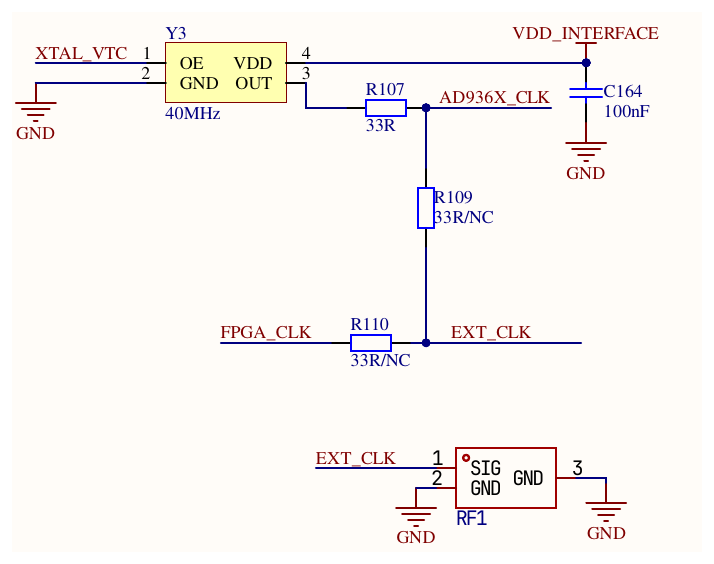
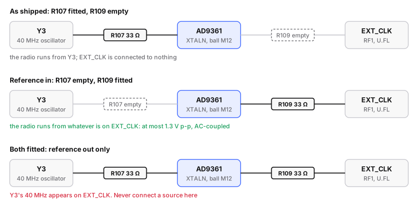
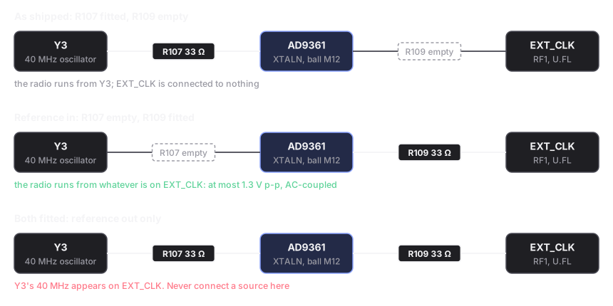
Move the 33 Ω resistor from R107 to R109. R107 joins the board's own
40 MHz oscillator (Y3) to the radio's reference line; R109 joins that line
to the EXT_CLK U.FL socket. As shipped, EXT_CLK is connected to nothing.
There is no software switch: the resistors are the switch.
R107 |
R109 |
The radio's reference | EXT_CLK |
|---|---|---|---|
| fitted | empty | Y3, 40 MHz (stock) |
nothing |
| empty | fitted | whatever is on EXT_CLK |
reference in |
| fitted | fitted | Y3 |
Y3's 40 MHz, out |
Never connect a source to EXT_CLK with both fitted
Two outputs then drive one line through 66 Ω. Measured: a HackRF CLKOUT
there changed nothing, because Y3 out-drives it.
What the reference must be
| Requirement | Why |
|---|---|
| 10 to 80 MHz | the AD9361's external-reference range |
| At most 1.3 V p-p, AC-coupled | XTALN sits in the chip's 1.3 V analogue domain; R109 alone provides no coupling capacitor and no attenuation |
| Running before the board boots | the driver locks the BBPLL once, at 1.4 s into boot |
clock-frequency in the device tree equal to it, unless it is 40 MHz |
the driver programs every PLL from that number; flash it with ./devkit flash --dtb-only |
A 3.3 V CMOS source needs a DC block and about 20 dB
XTALN is a high-impedance load, so a 50 Ω pad divides much less than its
rating: 6 dB leaves about 2.6 V p-p, 10 dB about 1.9 V p-p, 20 dB about
0.65 V p-p. From an open-circuit calculation; check the real swing on a scope.
HackRF One as the reference
Its CLKOUT is a 10 MHz, 3.3 V square wave, off after every power-up. Turn
it on before the Fishball boots, and set the device tree to <10000000>:
# run from: the PC the HackRF is plugged into
hackrf_clock -o 1      # CLKOUT on (10 MHz)
hackrf_clock -r 2      # on HackRF One r9, CLKOUT is Si5351 clock 2: "Up" means on
You should see: the radio start normally at boot, and the lock bits and measured frequency agree.
The radio does not start
With R107 removed and nothing driving EXT_CLK, the log shows
ad9361 spi0.0: Calibration TIMEOUT (0x5E, 0x80), then
probe with driver ad9361 failed with error -110; fishball-rf-quiesce
fails and iiod is held back, so nothing can transmit. Start the reference
before the board, or refit R107.
Two boards on one reference
One source, one output per board: a two-output GPSDO such as the Leo Bodnar LBE-1421 with both outputs set to 40 MHz, each through its own DC block and about 20 dB, keeps the device tree at 40 MHz. Not yet run on two boards; the set-up and the check that they really share it: beamform across two boards.
Reference: locking the board to an external reference,
with the photo of the pads, R110 (the FPGA's clock pin) and the Y3 pin 1 question.