# Four header pins that tick with the transmitted waveform
The base firmware can drive **four digital output pins whose every edge is
locked to a specific transmitted RF sample**. This page is the full reference:
how to use it, the pinout, the limits, how it is built and what has been
measured. The README has the [short version](../README.md#sample-locked-gpio-outputs).
You decide, sample by sample, what the pins do, and the delay between a pin
edge and the RF it belongs to is a fixed offset rather than a software
uncertainty. The feature costs no analog performance, because it uses bits the
radio discards.
The idea of passing the least significant bits of the transmit samples to the
GPIO pins came from **Akil0515** ([Telegram](https://t.me/Akil0515), listed in
[CONTRIBUTORS.md](../CONTRIBUTORS.md)).
**Contents**
- [The four bits nobody uses](#the-four-bits-nobody-uses): the idea
- [What "coherent" buys you](#what-coherent-buys-you): and what it does *not* mean
- [How to control it](#how-to-control-it): the switch, a complete Python example, GPIO mode
- [The pins](#the-pins): JP5 pinout, voltage, where the numbers come from
- [Limits](#limits)
- [How it is built](#how-it-is-built): datapath, module, wiring, cost
- [Building and flashing](#building-and-flashing)
- [Measured results](#measured-results): the hardware check, the logic-analyser figures
- [Notes for anyone extending it](#notes-for-anyone-extending-it)
---
## The four bits nobody uses
Three terms first, because they are easy to confuse:
- A **sample** is one number describing the signal at one instant. Transmitting
means handing the radio a long list of them.
- The **DAC** (digital-to-analog converter) is the chip block that turns each
sample into a voltage. Its **resolution** is how many bits of each sample it
reads.
- **DMA** (direct memory access) moves those samples from a buffer in RAM to
the radio without the CPU copying each one.
You hand the AD9361 **16-bit** samples; libiio, GNU Radio and every tool here
produce them. **The DAC is only 12 bits.** It takes the top 12 of your 16 and
ignores the rest:
```
# layout of one 16-bit transmit sample
your sample: b15 b14 b13 b12 b11 b10 b9 b8 b7 b6 b5 b4 │ b3 b2 b1 b0
└──────────── the DAC converts these ────┘ └─ discarded ─┘
```
ADI's HDL shows it: `axi_ad9361_tx_channel.v` does
`dac_data_out_int <= dma_data[15:4];`. The bottom four bits (the **low
nibble**) reach the FPGA and stop there. Nothing downstream reads them, so they
do not affect the transmitted signal at any sample rate reached the normal way.
The one path that would feed them to the DAC is the FPGA's ÷8 transmit
interpolator, which does not work on this board anyway; see [Limits](#limits).
This feature routes those four bits to four pins on the expansion header
instead of dropping them.
## What "coherent" buys you
**Coherent** here means a fixed, unchanging, known relationship in time between
two things. It does **not** mean simultaneous.
The pins carry bits `b0..b3` of a sample; bits `b4..b15` of the same sample
become RF. The pin is driven one FPGA clock after the sample leaves the DMA
unpacker, while the RF still has to cross the rest of the FPGA's transmit path,
the AD9361's digital filters, the DAC and the analog transmit chain. **So the
pins lead the RF**, by something on the order of a microsecond, depending on
how the filters are configured.
The lead is *constant*. It does not drift, it does not vary from sample to
sample, and it is the same on every run as long as the sample rate and filter
configuration stay the same. Measure it once, with a scope on a pin and another
on the RF or by looping the transmitter back into the receiver and
cross-correlating, and subtract it from then on. The offset has not yet been
measured on this board; see [Limits](#limits).
Software cannot do this. A GPIO toggled from Linux is tens of microseconds away
from the RF, and that delay changes from run to run and pulse to pulse; even a
kernel driver depends on the DMA queue depth. Here the offset is structural, so
it is a calibration constant rather than a source of error.
### What it is for
The motivating application is **multi-channel radar** (1 transmitter and 8
receivers, or 2 and 8). The transmit buffer in DDR holds the waveform, and the
low nibble of each sample carries, on separate pins:
| Pin | Typical use |
|---|---|
| `sample_gpio[0]` | **master clock**: a steady square wave the receivers clock from |
| `sample_gpio[1]` | **frame clock**: one pulse per pulse-repetition interval |
| `sample_gpio[2]` | **sync / trigger**: "the chirp starts *now*" |
| `sample_gpio[3]` | spare: a coded marker, a range gate, a T/R switch line |
Separate receiver hardware then samples with a timebase tied to the
transmitted waveform, which is what radar and MIMO (multiple-input
multiple-output: several antennas that must agree on phase) need.
**None of those roles is wired into the FPGA.** A pin's role is whatever
pattern you put in that bit.
---
## How to control it
There are two controls: a switch that hands the pins to the sample stream, and
the transmit buffer you write, whose low nibble is the pattern.
### Turning the bit-map on and off
```sh
# run on the board - resolve the device by name; the iio:deviceN index is not stable
D=$(for d in /sys/bus/iio/devices/iio:device*; do
[ "$(cat $d/name)" = cf-ad9361-dds-core-lpc ] && echo $d; done)
cat $D/tx_sample_gpio_en # 0 = GPIO, 1 = sample nibble
echo 1 > $D/tx_sample_gpio_en # on
echo 0 > $D/tx_sample_gpio_en # off
```
From your host, `iio_attr -u ip:192.168.2.1 -d cf-ad9361-dds-core-lpc
tx_sample_gpio_en 1` does the same (see [GPIO](gpio.md)).
Underneath, this is **bit 1 of the DAC core's `GP_CONTROL` register, AXI offset
`0xBC`**. Bit 0 of the same register is the interpolator bypass, so the
attribute read-modify-writes rather than assigning. On a build without
`patches/0007`, which adds the attribute, write the register through debugfs:
```sh
# run on the board, after setting D as above - older builds only
echo "0xBC 0x2" > /sys/kernel/debug/iio/$(basename $D)/direct_reg_access
```
The register resets to 0, so **the pins are ordinary GPIO at power-on** and the
feature is inert until you turn it on.
Changing the sample rate does not clear the flag. The driver's
`cf_axi_interpolation_set()` read-modify-writes only `BIT(0)`, so engaging or
bypassing the FPGA interpolation filter leaves bit 1 alone.
### Authoring the pin patterns
There is no "set pin 0 to clock mode" register. **The pattern is data.** You
build the transmit buffer and put the bits in it. A pin is a master clock
because that bit alternates; it is a frame marker because that bit pulses once
per frame.
**OR the nibble in last**, after every scaling, gain or format-conversion step.
Anything that multiplies your samples overwrites the bottom bits, because to
that code they are noise.
A complete program:
```python
# run on your HOST (not the board): pip install pyadi-iio numpy
import adi, iio, numpy as np
URI = "ip:192.168.2.1"
N = 4096 # buffer length in samples
# 1. Turn the bit-map on. It is an attribute of the DAC core rather than of
# the radio, so pyadi-iio does not expose it - reach it through libiio.
dac = iio.Context(URI).find_device("cf-ad9361-dds-core-lpc")
dac.attrs["tx_sample_gpio_en"].value = "1"
# 2. The radio. -89.75 dB is maximum attenuation: silent, and the pins still
# work, because the nibble never reaches the DAC.
sdr = adi.ad9361(uri=URI)
sdr.tx_enabled_channels = [0]
sdr.sample_rate = int(30.72e6)
sdr.tx_lo = int(2.4e9)
sdr.tx_hardwaregain_chan0 = -89.75
sdr.tx_cyclic_buffer = True # repeat the buffer forever -> a steady clock
fs = sdr.sample_rate
# 3. The RF you actually want to transmit, as int16.
n = np.arange(N)
sig = 0.5 * 2**15 * np.exp(2j * np.pi * 1e6 * n / fs)
i16 = sig.real.astype(np.int16)
q16 = sig.imag.astype(np.int16)
# 4. The digital side-channel: one bit per pin, as a function of sample index.
bit0 = (n % 2 == 0) # master clock: square wave at fs/2
bit1 = (n % 64 == 0) # frame clock: one sample high per 64
bit2 = (n == 0) # sync: one pulse at the top of the buffer
bit3 = np.zeros(N, dtype=bool) # spare
nibble = (bit0 | (bit1 << 1) | (bit2 << 2) | (bit3 << 3)).astype(np.int16)
# 5. LAST: clear the low nibble of I and drop the pattern in.
i16 = (i16 & ~np.int16(0x000F)) | nibble
# pyadi-iio casts real and imaginary straight to int16, so integer-valued
# complex input reaches the DAC bit for bit.
sdr.tx(i16.astype(np.complex128) + 1j * q16.astype(np.complex128))
print(f"streaming at {fs/1e6:g} MSPS; sample_gpio[0] is a {fs/2e6:g} MHz square wave")
```
The pins keep going until the buffer is destroyed. To stop and hand them back
to Linux:
```python
# run on your HOST, in the same session
sdr.tx_destroy_buffer()
dac.attrs["tx_sample_gpio_en"].value = "0"
```
[`tools/sample_gpio_clock.py`](../tools/sample_gpio_clock.py) is this program
with command-line arguments, the teardown wired to Ctrl-C, and an attenuator
check after the buffer opens.
- **`tx_cyclic_buffer = True` gives a continuous clock.** Author one period and
let the DMA loop it. Make the buffer length an exact multiple of your pattern
period, or there is a glitch at the wrap.
- **Only channel 0's I samples carry the nibble** in this build.
- **The analog cost is zero.** At full transmit power into a loopback, the
received tone was identical to within 0.04 dB with the nibble absent, present
in the data, and driving the pins at 30 MHz, and nothing appeared at the pin
frequencies down to the noise floor, about 64 dB below the carrier. The same
holds at low sample rates reached the normal way.
**The whole digital path works with the transmitter muted.** The nibble never
touches the analog chain, so at maximum TX attenuation (−89.75 dB) the pins do
exactly what you authored, with no meaningful RF leaving the port and no
antenna required. Setting the gain *before* streaming is not enough to
guarantee that: opening a TX buffer can itself raise the attenuator, because
the kernel restores a cached gain from the last stream when it unmutes (seen at
−61.5 dB on a board reading −89.75). `tools/sample_gpio_clock.py` and
`tools/tx-gpio-bitmap-check.py` read both attenuators back after the buffer
opens and stop if either moved; do the same in your own code.
### GNU Radio
The ordinary `complex float` flowgraph **does not work**. Every float sink
rescales on its way to int16, and rescaling destroys the low bits. GNU Radio
works only at `short` level end to end, with a sink that passes samples through
unscaled. It is usually easier to render the buffer with numpy, as above, or to
write a raw int16 file and transmit it directly.
### The pins as ordinary GPIO
With the flag clear, the four pins are EMIO GPIO bits 18–21 (EMIO: processor
GPIO lines routed out through the FPGA fabric; see [GPIO](gpio.md)). The Zynq
GPIO controller numbers its 54 MIO lines first and its 64 EMIO lines after
them, so `sample_gpio[0..3]` are controller lines **72–75**. That offset is a
property of the bitstream and does not change between kernels.
The lines are named in the device tree (patch `0008`), so they can be found by
name:
```sh
# run on the board - needs libgpiod-tools, see below
gpiofind sample_gpio0 # -> gpiochip0 72
gpioget $(gpiofind sample_gpio0) # read
gpioset $(gpiofind sample_gpio0)=1 # drive, with the feature off
```
> **`gpiofind` is not on the Debian rootfs.** Neither are `gpioinfo`, `gpioget`
> or `gpiodetect`: libgpiod-tools is not installed. `apt install gpiod` adds
> them. What works on **both** rootfs, with no packages, is the chip label:
>
> ```sh
> # run on the board - works on Buildroot and Debian
> for c in /sys/class/gpio/gpiochip*; do
> grep -q zynq "$c/label" 2>/dev/null && echo $(( $(cat "$c/base") + 72 ))
> done # -> 978 on 5.15, 584 on 6.12
> ```
The legacy sysfs interface is what the hardware check uses, because a shell
loop can drive it fast enough to sample a slow pattern:
```sh
# run on the board
BASE=$(cat /sys/class/gpio/gpiochip*/base | head -1) # 906 on 5.15, 512 on 6.12
N=$((BASE + 54 + 18)) # 978, or 584 on 6.12
echo $N > /sys/class/gpio/export
echo out > /sys/class/gpio/gpio$N/direction
echo 1 > /sys/class/gpio/gpio$N/value
```
The *sysfs* numbers depend on the kernel: **978–981** on the vendor's 5.15,
**584–587** on the 6.12 kernel in
[`firmware-modern/`](../firmware-modern/README.md), because the two kernels
place the controller base differently (906 against 512). `gpiofind
sample_gpio0` returns `gpiochip0 72` on both, which is why the tools here use
names.
### Reading the pins without fooling yourself
- **A pin's level does not tell you who is driving it.** With the flag clear
the fabric releases the pins and the pull-down holds them low, which is also
what the fabric drives for a zero nibble. To test the flag, stream *two
different* nibbles and check whether the pin follows the data. If it does,
the fabric owns the pin; if it reads the same either way, the fabric has let
go.
- **With `direction=out`, sysfs `value` returns what you wrote, not what is on
the pad.** EMIO bits routed to no pad at all read back identically, so a
readback in that mode proves nothing. Set `direction=in` to release the PS's
driver and let the pad level reach `gpio_i`. In bit-map mode the fabric keeps
driving the pin whatever the PS asks for, so `direction=in` plus a read shows
what the fabric is putting out. The hardware check also reads EMIO 22, which
is connected to nothing, as a control that must never go high.
---
## The pins
Four free single-ended 3.3 V I/O on connector **JP5**, unused by the stock
design. They are read off sheet 5 (`U1G`, "PL端BANK13") of the vendor schematic,
which is in this repository at
[`docs/vendor/`](vendor/7020_936x_SDR-schematic.pdf). Annotated crops of that
sheet and the two others that fix this assignment are
[below the pinout](#where-the-pin-numbers-come-from).
| Signal | Header net | JP5 pin | FPGA ball | FPGA pin name |
|---|---|---|---|---|
| `sample_gpio[0]` | `3V3_IO1` | 7 | **V10** | IO_L20N |
| `sample_gpio[1]` | `3V3_IO2` | 9 | **U9** | IO_L16P |
| `sample_gpio[2]` | `3V3_IO3` | 11 | **U10** | IO_L12N |
| `sample_gpio[3]` | `3V3_IO4` | 13 | **T9** | IO_L12P |
The bit number matches the header label, so `sample_gpio[0]` is the pin
silkscreened `3V3_IO1`.
JP5 also carries VCC1V8, VCC3V3 and VCC5V (pins 1, 3, 5) and four 1.8 V
differential pairs, which are where an I+Q widening would go. **Ground a probe
on pin 2 or 20.** The drawing is generated by `docs/img/make_jp5_pinout_svg.py`.
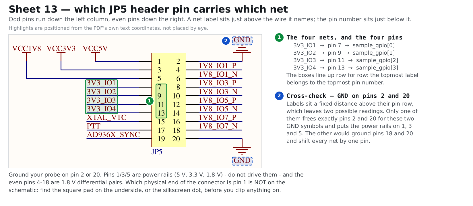
The pin *numbering* is straight off the schematic. Which end of the connector is
physically pin 1 is not: neither the schematic nor the board photo in this repo
shows it. Find the square pad on the underside, or the silkscreen dot, triangle
or "1", before you probe. Odd pins run down one column, even pins down the
other.
**Voltage and pull.** `LVCMOS33` is the right I/O standard: sheet 1 ties
`VCCO_13_1..4` (balls T8, U11, W7, Y10) to **VCC3V3**. `VCCO` is what a bank's
output drivers run from, so it fixes the voltage these pins swing to. Each pin
also carries `PULLTYPE PULLDOWN`, so an undriven pin reads a defined low. An
internal pull is safe here because each of the four nets appears exactly twice
in the whole schematic, once at the FPGA ball and once at JP5, so there is no
external pull, series part or ESD diode on them to fight. The pins idle *low*
rather than high because a sync line that floats high looks asserted to
whatever reads it.
The rest of the design declares `LVCMOS25` and `LVDS_25` on banks 34 and 35,
which the same sheet supplies from **VCC1V8**. That inconsistency is inherited
from ADI's stock Pluto constraints and is left alone because the board works
with it.
> **Do not guess these balls.** V11, W9 and V7 are adjacent bank-13 balls that
> look like plausible candidates, and the schematic marks all three **"no
> connect"**. V11 is the most misleading, because it is `IO_L20P`, the other
> half of the same differential pair as V10: adjacent ball, adjacent pin name,
> wired to nothing. Vivado accepts them without complaint and produces a clean,
> timing-met bitstream that drives three unconnected pads, because a wrong
> `PACKAGE_PIN` is not a build error.
#### Where the pin numbers come from
Where these numbers come from: the three vendor schematic sheets, annotated
The vendor's schematic is in this repository:
[`docs/vendor/7020_936x_SDR-schematic.pdf`](vendor/7020_936x_SDR-schematic.pdf).
Below are annotated crops of the three pages that fix the assignment, drawn
from it by
[`docs/img/make_schematic_figures.py`](img/make_schematic_figures.py); running
it regenerates them. Every highlight is positioned from the PDF's own text
coordinates, so a box cannot drift off the word it marks.
> Use that copy. The schematic the vendor publishes on their **GitHub** is a
> different board revision: 15 pages, no `JP5`, no `3V3_IO` nets, connectors
> numbered `J1`–`J12`. It does not describe this board. See
> [docs/vendor/](vendor/README.md).
**Sheet 5: which FPGA ball carries which header net.** Also marked are the
three balls that look right and are not: V11, W9 and V7 sit in the same bank,
next to the real ones, and the schematic marks all three *no connect*.

**Sheet 13: which JP5 pin carries which net.** Net labels sit a fixed distance
above their pin row, which allows two readings. Only one of them frees pins 2
and 20 for the two GND symbols and puts the power rails on 1, 3 and 5. The
other would shift every net by one pin.
**Sheet 1: bank 13's I/O supply, and why `LVCMOS33`.** The same ambiguity,
resolved the same way: only one reading puts the DDR3L memory bank on 1.35 V,
and that reading puts bank 13 on 3.3 V.

---
## Limits
- **Rate.** One nibble per sample, so the fastest a pin can toggle is half the
sample rate: 30.72 MHz at 61.44 MSPS. "Sample rate" means the rate of the
buffer *you* write. Every pattern is a whole-number division of that rate, so
arbitrary frequencies are not possible.
- **The pin-to-RF offset is not yet measured.** The pins have been measured
edge by edge; the fixed offset between a pin edge and its RF, the calibration
constant this feature exists to provide, has not. It needs the RF and a pin
on the same clock, for example an RF detector off a coupler in the transmit
line feeding a spare logic-analyser channel. Until then, treat it as
designed-for, not demonstrated.
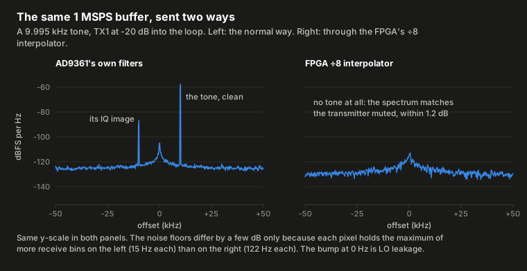
- **Do not engage the FPGA's ÷8 transmit interpolator.** It does not work on
this board, independently of this feature: a tone sent through it does not
come out at all. The received spectrum matched the muted transmitter to
within 1.2 dB of total power, while the same buffer sent the normal way
arrived clean. In this mode `tx_upack` is read at twelve times the buffer
rate instead of once per sample, which the pins show. The likely reason is in
the upstream block design, not in this repository's patches: `tx_upack` is
read on `interpolator valid OR dac_valid_i1`, and this board runs both
transmit channels (2R2T), so channel 1's direct path keeps emptying the
shared FIFO at the full rate. Why that gives silence rather than distortion
is not established. You only reach this mode by setting the DAC core's
`out_voltage_sampling_frequency` to one eighth of the AD9361's rate yourself.
pyadi-iio and the MCP server never do: below 2.083 MSPS they use the
AD9361's own filters instead, and the pins are correct at 1 MSPS that way.
- **The pins only move while a TX buffer is streaming.** Between streams the
last nibble is held. This firmware also mutes the transmitter and powers down
the TX synthesiser between streams (see
[Transmitter safety](transmitter-safety.md)).
- **I only, four pins**, unless you widen `NBITS`.
- **3.3 V LVCMOS**, single-ended, no series termination on the board. Keep the
wires short; buffer anything long.
- **Skew between the four pins is not constrained by timing analysis.** All
four switch within 1.5 ns of each other on a logic analyser, a figure that
includes the analyser's own channel skew. That is negligible against a 16 ns
sample period, but a picosecond-accurate instrument needs output constraints
and a re-run of implementation.
- **Long parallel wires cross-couple.** A pin toggling at 15–30 MHz put 20 ns
glitches on the pin next to it through a logic analyser's unshielded leads;
the board itself was clean. Keep wires short and give each signal its own
ground (JP5 pin 2 or 20) when a fast clock sits next to a slow signal.
- **Nothing validates your pattern.** The nibble is copied through untouched,
so a typo goes straight to the pins.
---
## How it is built
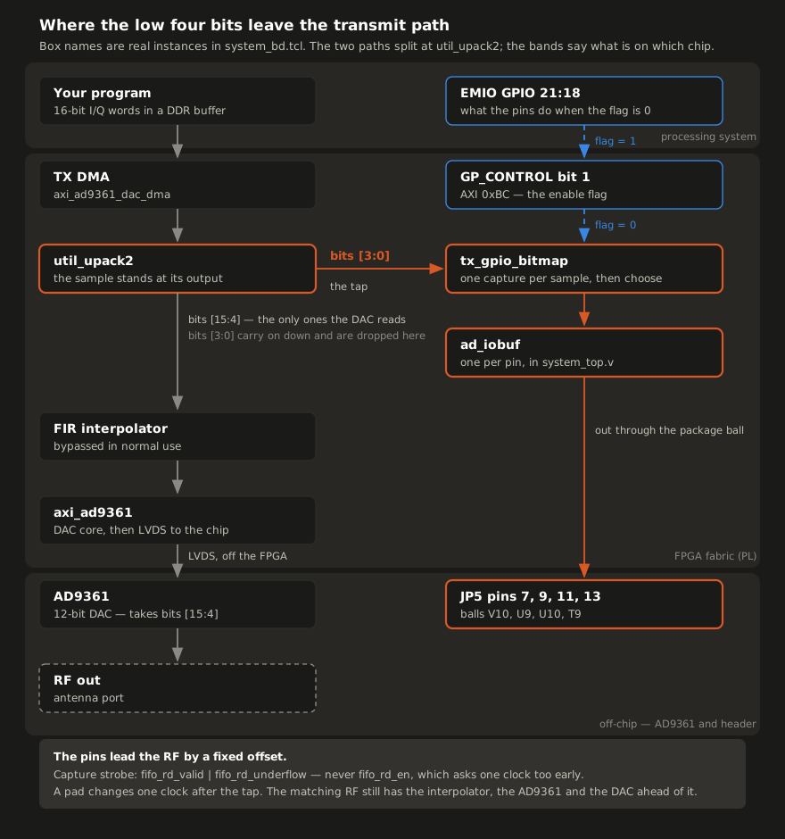
The FPGA does not *generate* anything. It **transports** whatever you author
into the low nibble to the pins, one nibble per sample. The four bits branch off
early, while the sample is still exactly the 16-bit word you wrote, and travel
to the pad on their own:
The same as text, with the enable flag and the ordinary-GPIO path shown:
```
# the transmit datapath and the nibble tap
DDR buffer ──DMA──> tx_upack ──┬── [15:4] ──> interpolator ──> AD9361 ──> RF
(16-bit samples) (unpacker) │ DAC
│
└── [3:0] ──> tx_gpio_bitmap ──> 4 header pins
▲ ▲
up_dac_gpio_out[1] ────┘ └──── EMIO GPIO 18-21
(the enable flag) (when flag = 0)
```
### Files
| File | What it is |
|---|---|
| `hdl/projects/pluto/tx_gpio_bitmap.v` | the module (~30 lines of logic) |
| `hdl/projects/pluto/system_bd.tcl` | block-design wiring: slices, the OR gate, EMIO widened 18 → 22 |
| `hdl/projects/pluto/system_top.v` | the `ad_iobuf` onto the four package pins |
| `hdl/projects/pluto/system_constr.xdc` | pin assignments and the CDC constraint |
| `firmware/sim/tb_tx_gpio_bitmap.v` | self-checking testbench, 2092 checks |
| `firmware/patches/0006-tx-sample-nibble-to-gpio.patch` | all of the above, applied by `setup.sh` |
| `firmware/patches/0007-tx-sample-gpio-iio-attribute.patch` | the `tx_sample_gpio_en` sysfs attribute |
| `firmware/patches/0008-name-the-sample-gpio-lines.patch` | the `sample_gpio0..3` line names in the device tree |
| `firmware/patches/0009-bitmap-flag-cdc-constraint-needs-from.patch` | the corrected CDC constraint |
The `hdl/` paths are under `firmware/src/`, which `setup.sh` creates.
### Where the nibble is tapped
The tap is `tx_upack/fifo_rd_data_0[3:0]`: **channel 0's I, straight out of the
DMA unpacker, before the interpolation filter.**
A FIR interpolator (a filter that raises the sample rate) mixes neighbouring
samples together. A tap downstream of it would put *filter output* on the pins
rather than the bits you wrote, and only while interpolation was engaged, so
the behaviour would change with the sample rate. Tapping the raw DMA word
delivers the pattern bit for bit whatever the rest of the transmit chain does,
and those bits are still exactly the ones the DAC discards.
`fifo_rd_data_1[3:0]` is channel 0's Q, the hook for a future I+Q widening.
### The capture strobe
The nibble is captured on `fifo_rd_valid | fifo_rd_underflow`, **not** on
`fifo_rd_en`:
- `fifo_rd_en` is a **request**: "give me a sample".
- `util_upack2` **registers** its output (`fifo_rd_data <= deinterleaved_data;`
in `util_upack2_impl.v`), so the requested word appears on the *following*
clock.
- `fifo_rd_valid` and `fifo_rd_underflow` are registered alongside the data.
Exactly one of them is high on the clock where the new word is at the output:
`valid` for a real sample, `underflow` for the zeros the unpacker substitutes
when the DMA has starved.
Capturing on `fifo_rd_en` would latch the *previous* sample: stable,
repeatable, and always one sample behind the DAC. Using the OR of the two
registered strobes also means that when the DMA underflows and the DAC is fed
zeros, the pins carry zeros too, so the pins are always the low nibble of what
the DAC got.
A per-sample strobe, rather than the clock, is needed because in **2R2T** mode
(both channels active) the datapath presents a new sample only every *second*
FPGA clock. Capturing on every clock would double the rate of every pattern: a
clock at half the sample rate instead of a quarter, a one-sample frame marker
arriving twice. This passes a back-to-back simulation and fails on hardware,
so the testbench checks it specifically and `run_sim.sh --mutate` proves that
check can fail.
### The module
```verilog
// in firmware/src/hdl/projects/pluto/tx_gpio_bitmap.v (ports only)
module tx_gpio_bitmap #(parameter integer NBITS = 4) (
input clk, rst, // l_clk and the datapath reset
input [NBITS-1:0] sample_in, // the raw DMA nibble
input valid_in, // "a new word is here NOW"
input flag, // up_dac_gpio_out[1]
input [NBITS-1:0] gpio_o_in, // EMIO GPIO, used when flag = 0
input [NBITS-1:0] gpio_t_in,
output [NBITS-1:0] pin_o, pin_t); // to an ad_iobuf at the top level
```
| `flag` | What owns the pins |
|---|---|
| `0` | **EMIO GPIO**: Linux drives them, tristate and all. The state at reset. |
| `1` | **the fabric**: `pin_o` = the registered nibble, `pin_t` = 0 (all driven) |
- **`NBITS` is a real parameter.** The testbench instantiates an 8-bit copy
alongside the 4-bit one, so the parameter is exercised. Widening to I+Q is a
parameter change plus four more pins.
- **The flag crosses two flip-flops.** Software writes it in the AXI clock
domain and the datapath reads it in the `l_clk` domain, a real clock-domain
crossing (CDC); the two-flop synchroniser keeps a metastable level out of the
fabric. A flag change therefore takes effect two clocks later.
- **Reset clears the held nibble**, so a datapath reset cannot leave a stale
bit pattern on the pins.
### Block-design wiring
All in `system_bd.tcl`, following the existing `interp_slice` template:
| Instance | What it does |
|---|---|
| `bitmap_sel` (`xlslice`) | bit **1** of `up_dac_gpio_out` → the enable flag. Bit 0 is already the interpolator bypass. |
| `nibble_slice` (`xlslice`) | `fifo_rd_data_0[3:0]` → the module's `sample_in` |
| `bitmap_valid_or` (`util_vector_logic`) | `fifo_rd_valid OR fifo_rd_underflow` → `valid_in` |
| `gpio_bitmap_o` / `gpio_bitmap_t` (`xlslice`) | EMIO GPIO bits **21:18** → the standard-GPIO inputs |
| `tx_bitmap` (module reference) | the module itself |
The PS7's `PCW_GPIO_EMIO_GPIO_IO` goes from **18 to 22** and the `gpio_i/o/t`
block-design ports widen to match, which gives the four pins their
ordinary-GPIO identity when the flag is clear. `system_top.v` adds an
`ad_iobuf` tying `pin_o`/`pin_t` to the package pins and feeds the pad inputs
back to `gpio_i[21:18]`.
### What it costs
Against a stock build of the same tree. Both columns were taken before patch
`0021`, so the baseline is the channel-0-only decimator: 72 DSP48s and 48 263
timing endpoints. The default build is now 94 DSP48s and 54 211 endpoints,
which shifts both columns equally and does not change the feature's own cost:
| | Stock | With the feature |
|---|---|---|
| Slice LUTs | 11 893 | **+3** |
| Slice registers | 20 851 | **+7** (4 nibble + 2 synchroniser + 1) |
| Bonded IOBs | 57 | **+4** |
| DSPs / block RAM | 72 / 2 | **no change** |
| Timing | WNS +0.214 ns | **WNS +0.205 ns**, 0 failing of 48 263 |
WNS is worst negative slack: how much margin the slowest path has. Timing is
met either way; differences of a few hundredths of a nanosecond between builds
are layout variation. The worst path is in ADI's DMA, not in this feature.
The enable flag's clock-domain crossing is constrained with
`set_max_delay -datapath_only` (patch `0009`), so Vivado does not time it as an
ordinary synchronous path with only 2 ns. In the routed design the crossing
reads `MaxDelay Path 4.000ns` and meets it with 2.46 ns to spare. See
[Notes for anyone extending it](#notes-for-anyone-extending-it) for why that
constraint needs both `-from` and `-to`.
---
## Building and flashing
`setup.sh` applies `0006` and `0007` with the rest, so a normal `build_all.sh`
includes the feature. There is nothing to opt into.
If you *modify* the module or its wiring, delete the Vivado project before
rebuilding. The block design is *generated* from `system_bd.tcl`, and a build
that finds an existing `pluto.xpr` reuses it, so wiring changes never reach the
fabric.
```bash
# run from: the repo root
cd firmware
rm -rf src/hdl/projects/pluto/pluto.{xpr,runs,gen,cache,hw,srcs,ip_user_files,sdk}
./scripts/build_all.sh --hdl-only
```
Simulate first. It takes a second and needs only `iverilog`:
```bash
# run from: firmware/
./sim/run_sim.sh # both custom modules, against golden models
./sim/run_sim.sh --mutate # and prove the tests can actually fail
```
The bitstream lives inside `BOOT.bin`, so `BOOT.bin` has to be replaced on the
card. `./devkit flash` does it over the network from a booting board, or use a
card reader. **DFU cannot do it.** See [Flashing the board](flashing.md).
---
## Measured results
### The hardware check
`tools/tx-gpio-bitmap-check.py` checks the feature on your board. It needs no
scope, no jumper and no antenna. TX attenuation is held at maximum throughout
and read back after every stream starts, which is safe because the nibble only
occupies bits the DAC discards.
```bash
# run from: the repo root, on your HOST
./tools/tx-gpio-bitmap-check.py ip:fishball.local
```
A passing run looks like this:
```
# output of tools/tx-gpio-bitmap-check.py (trimmed)
flag ON - each pin must carry its own bit of the nibble
0xF all high -> [1, 1, 1, 1] want [1, 1, 1, 1] control 0 ok
0x1 only bit 0 -> [1, 0, 0, 0] want [1, 0, 0, 0] control 0 ok
...
flag OFF - the fabric must let go, so the pins stop following the data
nibble 0x0 -> [0, 0, 0, 0] nibble 0xF -> [0, 0, 0, 0] released (pull-down holds them low)
timing - the pins must track the pattern at the rate the samples imply
bit0: 52 edges, period 499.6 ms, expected 499.3 ms, error 0.1% ok
bit1: 207 edges, period 124.8 ms, expected 124.8 ms, error 0.0% ok
RESULT: PASS
```
**How it reads the pins.** The path is **pad → the FPGA's input buffer →
`gpio_i[21:18]` → PS7 `EMIOGPIOI` → the GPIO controller's `DATA_RO` register →
sysfs**. In the routed design each pin is a real `IOBUF` primitive whose `I`
and `O` sit on *separate* nets (`sample_gpio_OBUF[n]` and
`sample_gpio_IBUF[n]`), so the value read is the input buffer sensing the pad,
not a loop-back of what was driven. With `gpio_o` set to 0, a floating pin
(before the pull-down was added) read 1, which an internal echo could not do. What this
does **not** establish: the PCB trace from the FPGA ball to the JP5 pin (taken
from the schematic), the actual voltage as opposed to which side of the logic
threshold it is on, and anything at edge resolution.
**The timing stage.** Static levels only prove the wiring. The timing stage
authors a square wave whose period is fixed by the buffer length and the sample
rate (one cycle per buffer on bit 0, four on bit 1), drops the sample rate to
the AD9361's minimum so sysfs can follow, and measures the period at the pin.
Both bits land on `N / fs` to within 0.1 %, simultaneously, with no drift over
a dozen seconds. The pins are clocked by the sample stream and nothing else; if
anything else drove them, the period would not track the sample rate. Sysfs
reads take milliseconds, so edge-level timing comes from the logic analyser
below.
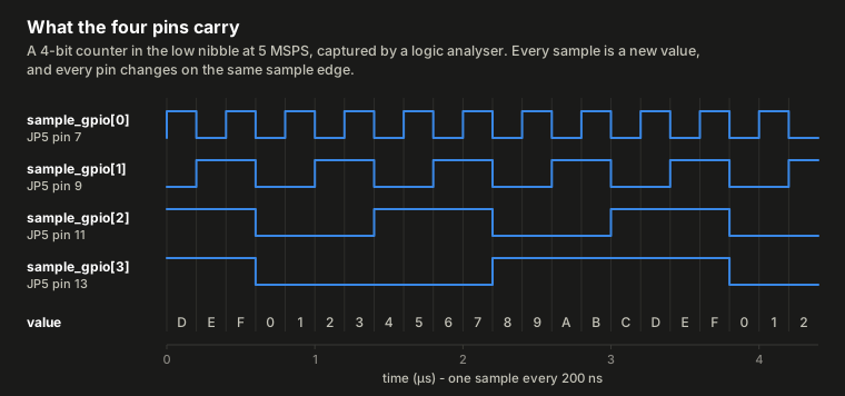
### On a logic analyser
A Saleae Logic 8 on the four pins, with the transmitter muted except where a
row says full power. The pattern was a counter, `nibble = n & 0xF`, so every
sample has a known value and one capture checks the bit mapping, dropped or
repeated samples, pin-to-pin timing and frequency together. With four channels
the analyser samples at 50 MS/s, 20 ns apart. The skew figure is finer than
that because the board's clock and the analyser's drift against each other, so
averaging over about 500,000 edges recovers sub-nanosecond timing.
At full transmit power the pins still swing cleanly between their logic levels:
And the transmitted signal does not change with them:
### Results
| Property | Result |
|---|---|
| Logic against a golden model | 2092 checks pass; 6 mutants all caught |
| Synthesis, implementation, timing | met; figures in [What it costs](#what-it-costs) |
| Pins on the intended balls | confirmed in the routed checkpoint |
| Ball assignments match the schematic | read off sheet 5 |
| Bank voltage supports LVCMOS33 | `VCCO_13` = VCC3V3, sheet 1 |
| Board boots with the feature | `BOOT.bin` built and flashed; AD9361 healthy afterwards |
| `tx_sample_gpio_en` sets the hardware bit | attribute and register `0xBC` agree |
| Idle level | reads 0 undriven (read 1 before the pull-down was added) |
| Nibble reaches the pins bit for bit | all four one-hot patterns, on hardware |
| Bit order | `sample_gpio[n]` = nibble bit `n` |
| Flag hands the pins back when cleared | yes |
| Pins track the pattern in time | two bits at once, 0.0–0.1 % period error |
| Every sample reaches the pins, in order | 1,002,706 consecutive samples, 0 errors (logic analyser) |
| Both transmit channels on (every-other-clock case) | 0 errors at 5 MSPS and at 61.44 MSPS |
| Both receive channels streaming at the same time | about 187 million samples, 0 slips |
| Full rate | pin 0 at 30.72 MHz from 61.44 MSPS, every sample present |
| Pin-to-pin skew | within 1.5 ns, same-direction edges |
| Electrical levels | 0.04 V / 3.28 V, 2–8 mV noise; ~30 mV idle |
| DMA underflow | pins go to zero on the very next sample |
| Effect on RF at full transmit power | identical to 0.04 dB, pins toggling or not |
| Ordinary Linux GPIO with the feature off | driven from `gpioset`, seen on the pads |
| Switching the feature mid-stream | one partial sample at the switch, nothing else |
| **Offset between a pin edge and its RF** | **not measured**: needs an RF detector on the analyser |
---
## Notes for anyone extending it
Four problems that simulation does not show:
- **Vivado infers bus interfaces from port names.** A vector beside a port
whose name ends in `_valid` becomes a data/valid *interface* pin, and
`ad_connect` then refuses to wire a plain slice output to it ("Cannot connect
non-interface to interface"). Hence `sample_in`/`valid_in` and
`(* X_INTERFACE_IGNORE = "true" *)` on every port.
- **An `.xdc` is a restricted Tcl dialect and does not accept `if`.** A guarded
constraint block is discarded whole, and the explanation appears in
`pluto.runs/*/runme.log`, *not* in the top-level build log. Check the run
logs, not just the build log.
- **A wrong `PACKAGE_PIN` is not an error.** Vivado places a port on a ball the
board leaves unconnected and reports perfect timing.
- **Clock-domain crossings are timed as if they were synchronous** unless a
constraint says otherwise, and that constraint can vanish.
`set_max_delay -datapath_only` needs both `-from` and `-to`. With only `-to`
it is an error (`Constraints 18-540`), and an `.xdc` drops the line without a
word in the build log. Patch `0006` wrote this feature's constraint with only
`-to`, so builds before patch `0009` timed the crossing as a 2 ns path (it
happened to pass). Check what was applied, not what you wrote: open the
routed design and run `report_timing -from -to `. The requirement must read `MaxDelay Path`, not two clock edges.
![JP5 pinout: a 2x10 header, with pins 7, 9, 11, 13 carrying sample_gpio[0..3] and grounds on pins 2 and 20](img/jp5-pinout-dark.svg)