# Two receivers that both survive decimation
When the FPGA's ÷8 decimator is engaged, upstream's block design filters only
channel 0, so channel 1 comes out aliased. Patch
`firmware/patches/0021-filter-both-receive-channels-by-default.patch` puts both
receive channels through the filter, for about six lines of Tcl and 22 DSP
slices. This page covers what the defect is, the before/after result, what the
patch changes and what it costs. Read it if you use both receivers at a
decimated rate, or build with upstream's wiring.
**It is the default.** Every build applies it. To build upstream's wiring
instead (channel 0 filtered, channel 1 straight through, 22 DSP slices back):
```bash
# run from: the repo root
STOCK_RX_FILTER=1 ./devkit build
```
`system_bd.tcl` prints which wiring it chose, and `./devkit verify` names it:
*decimator on BOTH RX channels* or *decimator on RX channel 0 only*. An empty
`STOCK_RX_FILTER=` counts as unset, not as yes. (The patch was previously the
opt-in `patches/optional/0004`.)
## The defect
Three facts in the stock block design combine badly:
1. **Only channel 0 is filtered.** Channel 0 passes through
`rx_fir_decimator`; channel 1 goes straight to `cpack` inputs 2 and 3.
2. **`cpack` captures everything on channel 0's timing.** Its write strobe,
`fifo_wr_en`, comes from `rx_fir_decimator/valid_out_0`. Channel 1's own
valid, `adc_valid_i1`, is connected to nothing.
3. **The decimator drops the rate by 8.** With it engaged, that strobe fires
once per eight input samples.
So with decimation engaged, channel 1 is sampled at one eighth rate **with no
anti-alias filter in front of it**. Everything outside ±Fs/16 folds onto it
([why](#why-a-decimator-needs-a-filter-at-all)), and it is also offset from
channel 0 by the filter's group delay. Stock, channel 1 is only a usable
receiver while the filter is bypassed.
Upstream shares this block design across a family of ADI boards, many of them
**1R1T** (one receiver, one transmitter). On those, "a filter on channel 0" is
a filter on the only channel there is, so the asymmetry only shows on a 2R2T
board like this one.
## Before and after
Conditions: `TX2A` → 20 dB attenuator → `RX2A`, tuned to 900 MHz. The converter
runs at 61.44 MSPS and the decimator is engaged, so the fabric delivers
7.68 MSPS, a window of **±3.84 MHz**. A tone generated inside the FPGA is swept
from 0.2 MHz to 20 MHz, and each level is compared with the same tone captured
with the decimator bypassed. The difference is the channel's **anti-alias
response**: how hard it pushes a tone down *before* that tone can fold into the
window.
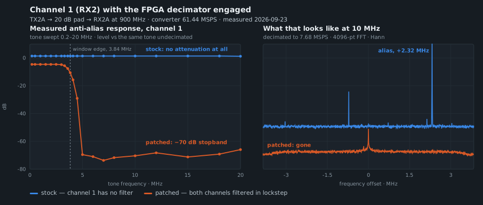
**Stock, the line is flat.** Channel 1 attenuates a 20 MHz tone exactly as
much as a 200 kHz one: not at all (+1.4 dB across the sweep). Every tone above
3.84 MHz arrives at full strength and lands *somewhere* in the window.
**Patched, both channels roll off together.** Flat at −4.6 dB through the
passband, −10.6 dB at the window edge, and an average of **−70.1 dB** past
5 MHz.
| Tone | Folds in at | Stock | With this patch |
|---|---|---|---|
| 1.00 MHz | 1.00 MHz, in band | +1.4 dB | −4.6 dB |
| 3.84 MHz | 3.84 MHz, the edge | +1.4 dB | −10.6 dB |
| 5.00 MHz | −2.68 MHz | +1.4 dB | **−69.6 dB** |
| 10.00 MHz | +2.32 MHz | +1.4 dB | **−70.4 dB** |
| 20.00 MHz | −3.04 MHz | +1.2 dB | **−66.0 dB** |
The right-hand panel is the 10 MHz row drawn as a spectrum. 2.32 MHz is exactly
10 − 7.68: the tone folded down by one output sample rate, which is what
aliasing does to anything above the window edge. Stock, that alias peaks at
**+18.75 dB**, indistinguishable from a real tone. Patched, the strongest bin in
the entire capture is the DC offset at **−50.92 dB** and the alias is not
visible above the noise: at least **69.7 dB of suppression**, which is the
filter's stopband applied to this channel.
With the decimator bypassed the two builds give the same result (the swept
reference levels agree within 0.05 dB over most of the range), so nothing is
lost in the undecimated case.
## What the patch does
The Tcl helper that builds the filter hierarchy already loops over its channel
count:
```tcl
# excerpt: projects/common/xilinx/adi_fir_filter_bd.tcl
for {set i 0} {$i < $n_chan} {incr i} {
ad_ip_instance fir_compiler $name/${filter_name}_${i} [ ... ]
...
}
```
So the fix asks for four channels instead of two, and wires the second pair
through:
```tcl
# excerpt: the patch's change to projects/pluto/system_bd.tcl
# ask for 4 (ch0 I/Q and ch1 I/Q) rather than 2
ad_add_decimation_filter "rx_fir_decimator" 8 4 1 {61.44} {61.44}
# feed channel 1 in
ad_connect axi_ad9361/adc_valid_i1 rx_fir_decimator/valid_in_2
ad_connect axi_ad9361/adc_enable_i1 rx_fir_decimator/enable_in_2
ad_connect axi_ad9361/adc_data_i1 rx_fir_decimator/data_in_2
ad_connect axi_ad9361/adc_valid_q1 rx_fir_decimator/valid_in_3
ad_connect axi_ad9361/adc_enable_q1 rx_fir_decimator/enable_in_3
ad_connect axi_ad9361/adc_data_q1 rx_fir_decimator/data_in_3
# and take cpack's inputs from the filter instead of from axi_ad9361
ad_connect cpack/enable_2 rx_fir_decimator/enable_out_2
ad_connect cpack/fifo_wr_data_2 rx_fir_decimator/data_out_2
ad_connect cpack/enable_3 rx_fir_decimator/enable_out_3
ad_connect cpack/fifo_wr_data_3 rx_fir_decimator/data_out_3
```
Both channels now share one `active` bit, one coefficient set and therefore one
group delay, so they stay sample-aligned. `cpack/fifo_wr_en` still takes
`valid_out_0`, which is correct because all four paths now produce output on
the same schedule.
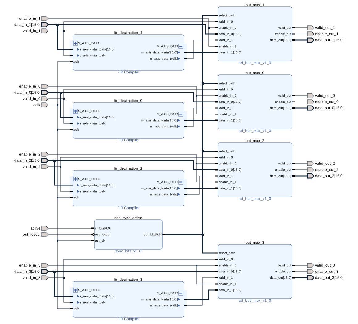
The resulting filter hierarchy, as Vivado draws it:
Four `fir_compiler` instances instead of two, four bypass muxes instead of two,
and one `cdc_sync_active` still driving every `select_path`, which makes the
two channels switch together rather than one at a time.
The whole block design, as Vivado draws it, is
[`img/bd-top.svg`](img/bd-top.svg); both drawings are exported with
[`img/make_bd_layout.sh`](img/make_bd_layout.sh).
## What it costs
| | `STOCK_RX_FILTER=1` | **Default** |
|---|---|---|
| DSP48 slices | 72 / 220 | **94 / 220** |
| Slice LUTs | 11,896 / 53,200 | 12,521 / 53,200 |
| Worst negative slack | +0.205 ns | **+0.215 ns** |
| Timing endpoints | 48,263 | 54,211 |
Two extra `fir_compiler` instances, about 11 DSP slices each. Timing is met
with slightly more margin than stock, and 126 DSP slices remain free.
## Using it
Nothing to do: `./devkit setup` applies it with the rest of the patch series.
To go back to upstream's wiring:
```bash
# run from: the repo root
# a block-design change means the Vivado project must go, or the build reuses it
rm -rf firmware/src/hdl/projects/pluto/pluto.{xpr,cache,gen,hw,ip_user_files,runs,sim,srcs,sdk}
STOCK_RX_FILTER=1 ./devkit build --hdl-only && ./devkit verify && ./devkit flash --boot-only
```
`./devkit verify` then reports `-> decimator on RX channel 0 only
(STOCK_RX_FILTER=1, upstream wiring)`; the default build reports `-> decimator
on BOTH RX channels (default)`.
Then engage the decimator and capture both channels:
```bash
# run on your HOST
iio_attr -u ip:192.168.2.1 -i -c cf-ad9361-lpc voltage0 sampling_frequency_available
# 61440000 7680000 <- always {converter rate, converter rate / 8}
iio_attr -u ip:192.168.2.1 -i -c cf-ad9361-lpc voltage0 sampling_frequency 7680000
# channel 0 is voltage0/voltage1, channel 1 is voltage2/voltage3
iio_readdev -u ip:192.168.2.1 -b 131072 -s 262144 cf-ad9361-lpc \
voltage0 voltage1 voltage2 voltage3 > both.bin
```
## What this does not fix
- **The transmit interpolator.** It is broken for a different reason:
`tx_upack/fifo_rd_en` is the OR of the interpolator's valid *and* channel 1's
DAC valid, so on a 2R2T board channel 1 drags the packer along at full rate,
and TX1 then emits nothing at all. See
[block-design.md](block-design.md#the-transmit-path). Do not engage it.
- **The shared coefficient file.** Receive and transmit both point at
`library/util_fir_int/coefile_int.coe`. Editing it changes both.
- **The ÷8 factor.** The driver offers exactly `{1, 8}`; a different rate would
build and be unreachable from software.
## Why a decimator needs a filter at all
Keeping one sample in eight *is* undersampling. It folds the whole captured
bandwidth into one eighth of it: eight slices stacked on top of one another,
noise included. The FIR empties the seven slices being discarded **before**
they can fold in.
That is also where the dynamic-range gain comes from: decimating by D buys
10·log₁₀(D) dB of signal-to-noise only *because* the filter removes the noise
in the bands being dropped. Without the filter the gain disappears along with
the usable signal. The anti-alias filter and the processing gain are the same
fact seen from two directions.